Download
1 / 20
200 likes | 354 Views
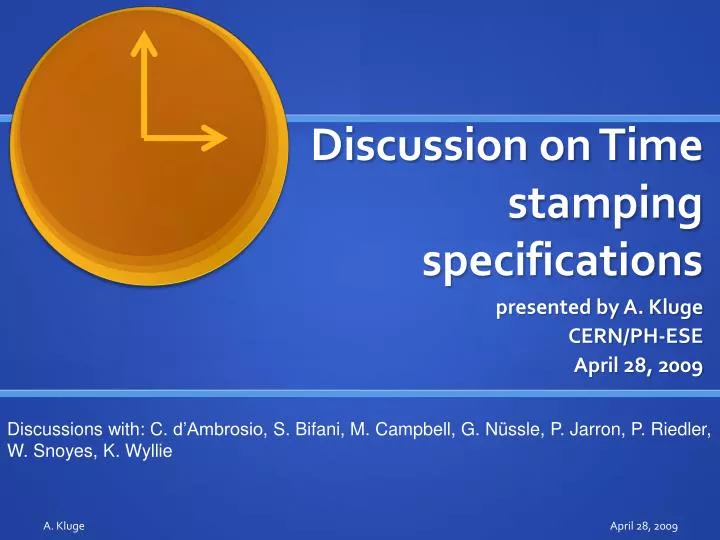
Discussion on Time stamping specifications. presented by A. Kluge CERN/PH-ESE April 28, 2009. Discussions with: C. d’Ambrosio , S. Bifani , M. Campbell, G. Nüssle , P. Jarron , P. Riedler , W. Snoyes , K. Wyllie. Outline. What are the specifications Which direction to go?

E N D
Discussion on Time stamping specifications presented by A. Kluge CERN/PH-ESE April 28, 2009 Discussions with: C. d’Ambrosio, S. Bifani, M. Campbell, G. Nüssle, P. Jarron, P. Riedler, W. Snoyes, K. Wyllie A. Kluge
Outline • What are the specifications • Which direction to go? • What are the options? A. Kluge
What are the Specifications ? • position resolution: 500 µmx 10 mm = 50 µmx 100 mm = 5 mm2 (pixels 20 x 20 µm2) • high segmentation better for analog: • low C and low I • high segmentation worse for digital: • more channels • time resolution: 1 – 2 ns • material budget: 0.4 – 0.6% (4% in 10 layers tracker) • occupancy: 10 (-50) hits /mm2/312 bx A. Kluge
Aim is to define Specifications A. Kluge
What can we do today? • Hybrid pixel detectors • < 100 µm Silicon sensor: 0.11 % Xo • <100 µm read-out chip: 0.11 % Xo • < 100 µm carbon fiber support: 0.10 % Xo • total 0.32 % X0 • + electrical connections & cooling • Power budget ~ 1 W /cm2 A. Kluge
What can we expect soon? • Hybrid pixel detectors • < 50µm Silicon sensor: 0.06 % XoIs signal large enough for time measurement? • < 50µm read-out chip: 0.06 % Xo • < 100 µm carbon fiber support: 0.10 % Xo • total 0.22 % X0 • + electrical connections & cooling • Power budget ~ 1 W/cm2 A. Kluge
Segmentation of pixels A. Kluge
Monolytic Active Pixel Sensors • People say: Thin 30 µm, very low material budget • Based on diffusion • Charge collection too slow for good time resolution • With depletion A. Kluge
Monolytic Active Pixel Sensors • With depletion A. Kluge
Monolytic Active Pixel Sensors • MAPS with depletion • 10 mW/cm2 aim of analog • present LHC detectors at > 1 W/cm2 • for timing precision charge collection must be constant regardless of where hits goes on the pixel A. Kluge
Signal & jitter & Si thickness • is silicon thick enough to get sufficient charge for timing resolution? • charge collection time / # electrons • 300 µm: 15 ns 22000 e- • 100 µm: 5 ns 7000 e- • signal collection for 200 µm Si (preliminary simulations by Simone Bifani) • at 80%: 0.714 ns +/- 0.241 ns • at 50%: 1.500 nsec +/- 0.274 ns • at 20%: 2.511 nsec +/- 0.409 nsec • 3D sensors…bump bonding A. Kluge
data rate & can pulsing be done • can power pulsing be done or is the read-out rate too high? • occupancy: 10 (-50) hits /mm2/312 bx • assume chip of: 10 mm x 10 mm and pixel size of 50 µmx 50 µm =>200 x 200 pixel = 40000 pixels = 16 bit addresstime stamping 1 bx out of 312 = 9 bitoccupancy => 10 hits/mm2 * 100 mm2 / 40000= 1000 / 40000= 2.5% • No trigger: Chip Data rate/ 312 bx => 1000 hits * 32 bit = 32000 bit32 kbit/20ms = 1.6 Mbit/sslow enough to daisy chain32 kbit/312 bx= 200 Gbit/s • No trigger: Data rate /cm2 = 1.6 Mbit/scontinous A. Kluge
Cooling • Industry will reach power limit? • Will we be able to benefit from this? • Micro channel cooling A. Kluge
Micro channel cooling Si: 31 x 31 x 1 mm3 surface roughness 160 nm 134 parallel channels: l = 20 mm, w = 67 µm, h = 680 µm, separation 92 µm 255 W/cm2 A. Kluge
will smaller CMOS feature size help for the power consumption • P = C * f * U2 • gate leakage in 65 nm = 1nA/µm2 A. Kluge
Alternatives • Micro channel plates + Pixel chips A. Kluge
Scintillating Fibers • short fibers (~ 10 cm) -> signal spread & time of flight small (0.5ns) • Silicon photo multipliers (SiPM) • Dead time recovery/Occupancy A. Kluge
Small diameter scintillating fibres consist of bundles of hexagonal fibres (typ. 60 µm dia., 2.5 mm bundle size) 1 mm diameter scintillating fibres Can be packed in ribbons to ensure uniform efficiency and high precision 1 mm 10 to 25 hits 2.5 mm 5 to 25 hits Both arrangements correspond to ~0.6 % Xo, 0.3 % λi, 0.45 % γ conv. length, 100 μrad mult. scatt. angle for a 10 GeV/c particle For their rad. hardness, the rule of thumb is ~10 kGy per year. LHCb Brainstorming - Scintillating Fibres for Tracking C. D’Ambrosio, CERN
Conclusion • In order to select the proper approach we need to know the needs, where are we in the parameter space? • Parameters in order of importance: A. Kluge
Monolytic Active Pixel Sensors A. Kluge