Download
1 / 12
120 likes | 125 Views
This lecture covers the process of transitioning from pseudocode and interface to a corresponding block diagram in RTL design methodology. Topics include the structure of a typical digital system, hardware design with RTL VHDL, steps of the design process, and implementation and testing techniques.

E N D
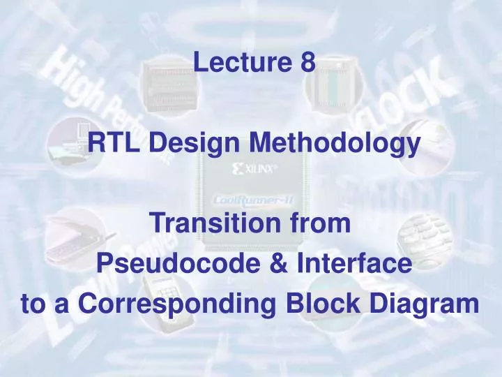
Lecture 8 RTL Design Methodology Transition from Pseudocode & Interface to a Corresponding Block Diagram
Required reading • P. Chu, FPGA Prototyping by VHDL Examples • Chapter 6, FSMD • S. Brown and Z. Vranesic, Fundamentals of Digital Logic with VHDL Design • Chapter 10.2, Design Examples ECE 448 – FPGA and ASIC Design with VHDL
Structure of a Typical Digital System Data Inputs Control & Status Inputs Control Signals Datapath (Execution Unit) Controller (Control Unit) Status Signals Data Outputs Control & Status Outputs
Hardware Design with RTL VHDL Interface Pseudocode Datapath Controller Block diagram State diagram or ASM chart Block diagram VHDL code VHDL code VHDL code
Steps of the Design Process • Text description • Interface • Pseudocode • Block diagram of the Datapath • Interface with the division into the Datapath and the Controller • ASM chart of the Controller • RTL VHDL code of the Datapath, the Controller, and the Top Unit • Testbench of the Datapath, the Controller, and the Top Unit • Functional simulation and debugging • Synthesis and post-synthesis simulation • Implementation and timing simulation • Experimental testing
Steps of the Design ProcessPracticed in Class Today • Text description • Interface • Pseudocode • Block diagram of the Datapath • Interface with the division into the Datapath and the Controller • ASM chart of the Controller • RTL VHDL code of the Datapath, the Controller, and the Top Unit • Testbench of the Datapath, the Controller, and the Top Unit • Functional simulation and debugging • Synthesis and post-synthesis simulation • Implementation and timing simulation • Experimental testing
Statistics example
Circuit Interface clk done reset n n dout Statistics din 2 dout_mode go
Pseudocode no_1 = no_2 = no_3 = sum = 0 for i=0 to k-1 do sum = sum + din if din > no_1 then no_3 = no_2 no_2 = no_1 no_1 = din elseif (din > no_2) then no_3 = no_2 no_2 = din elseif (din > no_3) then no_3 = din end if end for avr = sum / k
din n n n en1 reset en rst n+m clk A gt1 clk n+m no_1 A>B n esum B n reset en rst clk 1 0 s2 clk sum n+m en2 reset enc en reset en rst rst clk clk clk clk A gt2 no_2 m A>B n n+m n B i 1 0 s3 >> m = k-1 en3 reset en rst clk n A gt3 clk A>B avr no_3 zk n B no_3 no_2 no_1 n n n dout_mode 00 01 10 11 2 n dout Block diagram of the Datapath
Interface with the division into the Datapath and the Controller din dout_mode clk reset go n 2 gt1 gt2 gt3 Datapath Controller zk en1 en2 en3 esum enc s2 s3 n dout done