Download
1 / 28
280 likes | 391 Views
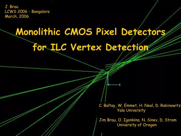
J. Brau LCWS 2006 - Bangalore March, 2006. C. Baltay, W. Emmet, H. Neal, D. Rabinowitz Yale University Jim Brau, O. Igonkina, N. Sinev, D. Strom University of Oregon. ILC Vertex Detectors. GLD. LDC. S i D. Z= 6.25cm. SiD Vertex Layout. 5 barrel layers 4 end disks. 5 Tesla. R

E N D
J. Brau LCWS 2006 - Bangalore March, 2006 C. Baltay, W. Emmet, H. Neal, D. Rabinowitz Yale University Jim Brau, O. Igonkina, N. Sinev, D. Strom University of Oregon J. Brau LCWS 2006 March, 2006
ILC Vertex Detectors GLD LDC SiD J. Brau LCWS 2006 March, 2006
Z= 6.25cm SiD Vertex Layout 5 barrel layers 4 end disks 5 Tesla R [cm] SiD00 Design drivers: Smallest radius possible Clear pair background Seed tracks & vertexing Improve forward region Role: Z [cm] J. Brau LCWS 2006 March, 2006
SiD Vertex Detector • BARREL • 100 sensors • 1750 cm2 • FORWARD • 288 sensors • 2100 cm2 J. Brau LCWS 2006 March, 2006
ORIGINAL IDEA –Hierarchical array (Macro/Micro) w/SARNOFF J. Brau LCWS 2006 March, 2006
Summary • Investigation of Hierarchical Approach • Macro/Micro Hybrid (50 um ~5 um) Macro only, reduced to 10-15 um pixel • Completed Macropixel design • 645 transistors • Spice simulation verified design • TSMC 0.18 um -> 40-50 um pixel • Next phase under consideration • Complete design of Macro pixel • Deliverable –tape out for foundry (this year) • Future • Fab 50 um Macro pixel design • Then, 10-15 um pixel (Macro pixel) J. Brau LCWS 2006 March, 2006
Background Hits Dominate Vertex Detector • Events of interest are relatively rare – • less than 1 Hertz. • hit rate in Vertex Detector dominated by background. • Detailed calculations yield an expected background estimate of 0.03 hits/mm2/Bunch Crossing • However, with considerable uncertainty on this level of background. • Difficult calculation. • Background will depend on final choice of collider design details. J. Brau LCWS 2006 March, 2006
The Macropixel Array is Critical • Big Pixel size (initially 50 umx 50 um) limits the tolerance to higher backgrounds. • Therefore important to strive to reduce Big Pixel size. • Reducing the Big Pixel size to 10 umx 10 um (or even15 umx 15 um)makes detector much more tolerant to backgrounds. • Macropixel Array (Big Pixel size) of 10-15 um might not need complement of micropixels • simplified design of single layer of "Macropixels" • with time information • Might not need analog information. J. Brau LCWS 2006 March, 2006
What Limits the Macropixel Size • Compress Big Pixel size, retaining storage of hit time information for 4 hits/pixel/bunch-xing • Area needed with present technology (0.25 um?) • Comparator/counter/latch, etc., circuit • Storage of up to 4 hits, i.e., 14 bits x 4 deep • Process Technology - how does pixel size scale as process technology goes 0.25 um, 0.13 um, etc? • What do you need to go to 10 um x 10 um pixels? • Can you estimate the progress of this technology? • What's available today? • Much more interesting - what will be available - 5 years from now when we need to fabricate the actual devices?; • How much does it help to reduce max number of time stamps stored to 2 or 3? J. Brau LCWS 2006 March, 2006
Readout Procedure and Speed • First, some numbers: • Consider chips 22 mm x 125 mm = 2750 mm2 – • Total no. of 10 um x 10 um pixels = 27.5 x 1O6 pixels/chip – • Total hits .03 x 2820 x 2750 = 2 x l05 hits/chip/bunch train • How long does it take to interrogate a pixel to see if it has a hit (presumably look of a single bit flag?) • How long does it take to read out one hit pixel • X info (up to 2200) - 12 bits + parity = 14 bits • Y info (up to 12500) - 14 bits + parity = 16 bits • Time (up to 3000) - 12 bits + parity = 14 bits 44 bits total • 2 x 10⁵ hits/chip x 44 bits/hit / 50 MHertz = 176 msec • Might divide each chip into parallel readout streams (10-20) to accommodate higher background rates? J. Brau LCWS 2006 March, 2006
Charge Spreading • Important to minimize charge spreading • pixel size sets scalethat would reduce need for analog information. • How small can we keep the charge spreading? • Thickness of expitaxial layer - 10 to 15 um • Possible approach - full depletion of epitaxial layer • requires high resistivity? - few kohm-cm? or less? • Depletion voltage, field in epilayer? J. Brau LCWS 2006 March, 2006
Read Noise • Minimum ionizing particle leaves 88e- /micron in expitaxial layer • 10 umthick epi x 88e-/um = 880 electrons • GOAL - signal to noise of 10 to 20 • Can we keep read noise below 50 e- or so? • This consideration determines thickness of the exitaxial layer. J. Brau LCWS 2006 March, 2006
Power Consumption • Keep power to ~100 millwatts/chip (goal) ~4 mW/cm2 • Trade-off noise with power • Make design choices which optimize noise/power tradeoffs J. Brau LCWS 2006 March, 2006
Power Dissipation Analysis • Additional 67- to 100-fold reduction expected by power cycling analog components (0.37 – 0.55 uW) J. Brau LCWS 2006 March, 2006
Other Considerations • Dark Current • Keep it small • Sarnoff – will reset array on each bunch • Should not be a problem • Operating Temperature • Sarnoff expects modest cooling (<0C adequate) • Device Thickness • Thinning below 50 um looks feasible • B Field – Lorentz angle J. Brau LCWS 2006 March, 2006
Spice Model Verification of Design J. Brau LCWS 2006 March, 2006
SARNOFF Response to Question on Future Technology Roadmap: Macropixel size estimation vs. Mixed-signal Process Technologies J. Brau LCWS 2006 March, 2006
CONCLUSION • Completed macropixel design • 645 transistors • Spice simulation verifies design • TSMC 0.18 um -> 40-50 um pixel • Next phase under consideration • Complete design of macro pixel • Deliverable –tape out for foundry • Future • Fab 50 um pixel chip • Then, 10-15 um pixel J. Brau LCWS 2006 March, 2006
EXTRAS J. Brau LCWS 2006 March, 2006
Power Reduction Method • Activate the Detector and the Comparator during the Bunch Train and deactivate rest of the time • Power Reduction Ratio = 1/67 to 1/100 (0.552 mW to 0.37 mW) J. Brau LCWS 2006 March, 2006