Download
1 / 16
170 likes | 405 Views
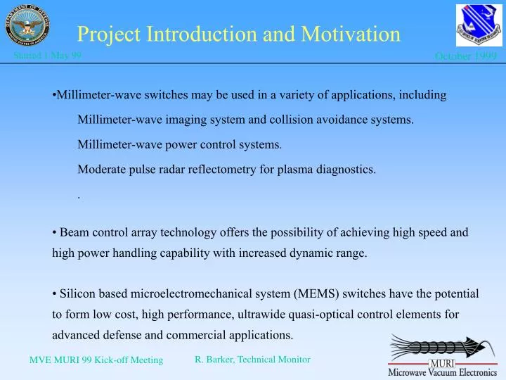
Project Introduction and Motivation. Millimeter-wave switches may be used in a variety of applications, including Millimeter-wave imaging system and collision avoidance systems. Millimeter-wave power control systems . Moderate pulse radar reflectometry for plasma diagnostics. .

E N D
Project Introduction and Motivation • Millimeter-wave switches may be used in a variety of applications, including • Millimeter-wave imaging system and collision avoidance systems. • Millimeter-wave power control systems. • Moderate pulse radar reflectometry for plasma diagnostics. • . • Beam control array technology offers the possibility of achieving high speed and high power handling capability with increased dynamic range. • Silicon based microelectromechanical system (MEMS) switches have the potential to form low cost, high performance, ultrawide quasi-optical control elements for advanced defense and commercial applications.
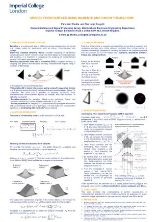
Switch Array SwitchedMmwave Output CW Mmwave Input Matching Plate Matching Plate Bias Microstrip Wilkison Power Divider Microstrip to CPW Transition Wirebond from Bias Board to GaAs Wafer High Speed Switching System Design E • The high speed switch consists of a quasi-optical beam control array, matching system, and high speed bias circuitry. • Quasi-optical power combining techniques are utilized to obtain high output power by combining the power of thousands of diodes. • The control speed is limited by three factors: the quasi-optical array physical dimensions, bias circuitry, and diode grid layout.
Equivalent Circuit Model of the Diode Grid Unit Cell Equivalent Circuit for Diode Grid Unit Cell SEM photo of Unit cell E-Field Distribution of Top View of Schottky Varactor
High Speed Switch Array with Bias Control Board
V-K Trans. K-V Trans BWO Atten. Directional Coupler Isolator Diode Detector Power Detector Overmode Waveguide Mounting Fixture Frequency Meter Sampling Oscilloscope Pulse Circuit Signal Generator Signal Trigger High Speed Beam Control Switch Testing Setup
High Speed Switch Testing Results Comparison Between Measured and Simulated Contrast Ratio • <1.5 dB insertion loss and 16.8 dB on/off contrast ratio measured at 60 GHz.The switch fall time is <127 psec, rise time is 168 psec with pulse width (FWHM) 317 psec limited by bias pulse. • > 10 dB on/off contrast ratio for the frequency band from 55 GHz to 66 GHz.The measured results are very close to the simulation results.
New High Speed Switch Performance • High speed, monolithic millimeter wave switch arrays, which will operate at V-band and W-band, have been designed and are being fabricated • In the new class high speed switch system, a new 1:8 wilkinson power divider and a new optimized overmoded K-band mounting fixture will be used. • The grid switch array size is 0.4 x 1 cm2. There are around 400 Schottky varactor diodes on the wafer, and it can handle power levels in excess of 1 W. • Lower insertion loss and higher contrast ratio is expected: V-band switch array: < 1 dB insertion loss and 27 dB ON/OFF contrast ratio. W-band switch array: < 2.5 dB insertion loss and > 25 dB ON/OFF contrast ratio.
Introduction: Microelectromechanical System (MEMS) • MEMS stands for Micro-Electro-Mechanical System, where the physical dimensions are on the order of a few or tens of microns. • There are two advantage of RF MEMS devices compared to traditional semiconductor devices: • a. Electromechanical isolation • b. Power consumption • Developments in MEMS technologies have facilitated exciting advancements in the fields of sensors (accelerometers and pressure sensors), micromachines (microsized pumps and motors), and control components (high definition TV displays and spatial light modulators).
Microwave / Millimeter Wave MEMS Switch Operation • The MEMS switch consists of two metal plates, a fixed base plate and a movable thin film membrane. • Electrically, the MEMS switch is a nonlinear function of the DC bias applied to the switch. • Through the application of a DC electrostatic field, the MEMS membrane is attracted towards a metalized bottom contact.
SEM Photo of MEMS Switch • The top metal with holes is a movable membrane, which is supported by Al post. • The holes are employed to etch the sacrificial layer using a plasma etcher. The unit cell size is 1200 x1200 µm2, and membrane is 120 x120 µm2.
MDS Simulation of MEMS Power Control Array • The MDS simulation tool has been used to simulate the MEMS switch array. • The contrast ratio is > 20 dB over a 20 GHz bandwidth.
LC Circuit LC Circuit Transmission Line Transmission Line Design of MEMS Tunable Filters Equivalent circuit of the Tunable Filter QO MEMS Tunable Filter System MEMS Tunable QO filter consists of sevearl pieces, an LC resonant circuit is fabricated on each of the wafer surfaces.
Simulation Result of W-band Tunable Filter • W-band tunable filter can tune ~30 degree phase shift From 30GHz---40GHz.
Ongoing Activities • A new class of GaAs based V-band and W-band high speed monolithic millimeter wave switch array has been designed and is being fabricated. • MEMS Switch array technology is being developing. MEMS based quasi-optical arrays will be employed as quasi-optical power control, quasi-optical phase shifters, and tunable quasi-optical filters.