Download
1 / 9
90 likes | 213 Views
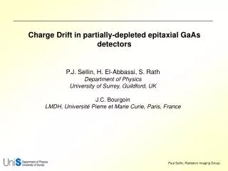
Charge collection in X-ray pixel detectors based on SI-GaAs doped with Cr. G.I.Ayzenshtat a , M.V.Bimatov b , O.P.Tolbanov c , A.P.Vorobiev d a Science & Production Enterprise “Semicond. Dev. Research Inst”, Tomsk, Russia b Tomsk State University, Tomsk, Russia

E N D
Charge collection in X-ray pixel detectors based on SI-GaAs doped with Cr G.I.Ayzenshtata, M.V.Bimatovb, O.P.Tolbanovc, A.P.Vorobievd a Science & Production Enterprise “Semicond. Dev. Research Inst”, Tomsk, Russia b Tomsk State University, Tomsk, Russia c Siberian Physical Technical Institute, Tomsk, Russia d State Science Center “High-Energy Physics Institute”, Protvino, Russia
Introduction The charge collection in a pixel detector and output current shape were investigated for LEC SI-GaAs in the works by P.J.Sellin, M.G.Bisogni and others. The purpose of our work is to simulate a current and charge signal in the pixel detector after X-ray absorption at various positions in the detector for GaAs compensated by Cr. This material distinctive features are: • an uniform electric fielddistribution through the detector; • much longer lifetime of an electronthan of a hole (τe >> τh). The material characteristics: The mobility and lifetime values of charge carriers are: µh = 200 cm2/Vs, µe = 1500 cm2/Vs τh 0.2 ns, τe10ns, The electron velocity depends nonlinearly on the electric field strength: ve = µeE when E < 5 kV/cm; ve = 7.5•106cm/s when E > 5 kV/cm
where z is the perpendicular coordinate, h is the detector thickness. , k=0,±1,±2,… A Formula for the pixel current The following formula was obtained for calculation of the current induced on a pixel by a moving charge: (1) where R=D/2 is half pixel size, x and y are the horizontal coordinates, q and v are the charge value and the charge velocity respectively; function f is: (2) D=100µm z thickness=500µm x x y
The currents induced on irradiated and neighbouring pixels (the capture was neglected) µe =1500 cm2/Vs , µh = 200 cm2/Vs The side view of the detector: the neighbouring pixel the irradiated pixel z D=100µm thickness=500µm • The conclusion: The negative current pulse arises • in the neighbouring pixel
The current induced on the pixel tacking into account the capture lifetimes of the charge carriers: τh 0.2 ns τe10ns • Pixel contacts should be anodes (for SI – GaAs:Cr)
Dependences of CCE on the photon absorption depthfor events occurring under the pixel center z 500µm 0 • Pixel contacts should be anodes (for SI – GaAs:Cr)
The dependences of CCE on the photon absorption depth for events occurring at various distances from the pixel center • Signal induced on the next nearest pixel is negligible. the examined pixel the examined pixel z z x=50µm x=100µm 0 0 x x
Mean charge collected on the pixel as a function of the detector thicknessThe charge averaged over all photons incident on the detector cell • There is an optimal detector thickness for the mean collected charge. • Its value is determined by the photon energy and the drift length of charge carriers.
Conclusions • The formula for the current induced on the square pixel by a moving charge was obtained. • The negative current pulse arises in the neighbouring pixel. • The pixel contacts should be anodes in the detector based on SI-GaAs compensated by Cr. • There is an optimal detector thickness for the mean collected charge. Its value is determined by the photon energy and the drift length of charge carriers.