Download
1 / 36
850 likes | 2.68k Views
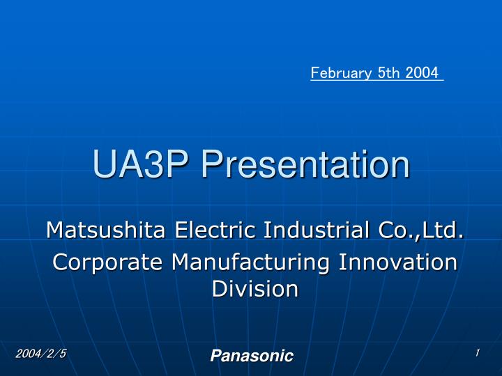
February 5th 2004 . UA3P Presentation. Matsushita Electric Industrial Co.,Ltd. Corporate Manufacturing Innovation Division. Ultrahigh Accurate 3-D Profilometer(UA3P). 1. Appearance 2. Specification s 3. The characteristic of Technologies 4. Measurement Applications

E N D
February 5th 2004 UA3P Presentation Matsushita Electric Industrial Co.,Ltd. Corporate Manufacturing Innovation Division Panasonic
Ultrahigh Accurate 3-D Profilometer(UA3P) 1. Appearance 2. Specifications 3. The characteristic of Technologies 4. Measurement Applications 5.The analysis of the measurement data 6. Traceability system 7.Closure Panasonic
1. Appearance. The measurement range • UA3P type4 • 100*100*35mm • UA3P - type5 • 200*200*45mm • UA3P - type6 400*400*90mm 1550 1350 1200 UA3P-5 Panasonic
Overview Development of the Profilometer and Products Created Form Talysurf (Taylor & Hobson) Measuring Devices Developed Profilometer ~100mm 2nd Generation Atomic Force Probe 3-D Profilometer (available commercially) 3-D Profilometer Θ - The measurement accuracy (5 µm) is too low for lens measurement. - The measurement force is large : 150 gf SAG L Accuracy : 0.01 μm Measurement plane tilt angle : up to 60o Measuring force : 30 mgf Existing Measuring Equipment - Measurement accuracy : 0.5 μm, for only one axis - Measurement plane tilt angle : up to 35o Introduction to Giga-Bit wafer measurement Slip Stylus 1st Generation Optical 3-D Profilometer Interferometer Atom - Can measure only spherical surfaces. - Measurement accuracy : 0.1 μm - Measurement of a high-tilt plane available for only one axis, up to 45o. Equipped with software for user-definable free-form surface object Measured object Year 1978 1986 1994 2002 Optical Components Lens array for optical communication Spherical lens An Aspherical lens could not be made due to the lack of an adequate means of measurement. First production of aspherical lens Tilt angle : up to 37 High-resolution aspherical lens Tilt angle : 55o Wafer for large capacity semicon-ductors Head mount display CD Car navigation system Memory Devices DVD recorder 2001 Product of the Year awarded by Nikkei LBP Realization of CD players and DVC equipped with an aspherical lens Analog Records Game machine (PlayStation 2) DVD player Stepper, Wafer Camcorde Input Devices Increased need for projection TV systems in the U.S. Cellular phones equipped with a lens Panasonic Camera Aspherical bifocal glasses Digital camera PC with a CD/DVD drive Spherical glasses DVC
The present technology has led to the advent of nanotechnology or free-form surface components, which could not previously be developed or manufactured because of the lack of a suitable means of measurement. Overview Axis for Freedom of Form Machine Industry Area Optoelectronics/Nanotechnology Area Flat/Spherical Surfaces --> Free-form Surfaces mm 1000 Area of Ultrahigh Accuracy Area Covered by Existing 3-D Profilometers Steppers Fields where only UA3P is capable of the required degree of measurement accuracy Projection TV sets 100 Semiconductor wafers Laser Printers Accuracy required by commonly used machinery LSI Eyeglasses Camcorders 10 Sizes/Measurement Range Axis Mechanical parts Precision mechanical parts Instant cameras Optical discs Line indicating Measurement Accuracy/Range = 10-5 The upper or right side of this line is the area of ultrahigh accuracy. 1 Optical communication 3-D measurement unattainable with optical microscopes Micro-lens CCD 0.1 Micro machine SEM, STM, AFM Area Covered by UA3P 0.01 1 nm 1mm 100μm 10μm 1μm 100nm 10nm Accuracy Axis Relationship between Industry Segments and Accuracy Panasonic
2. Specifications Panasonic
3. The characteristic of technology Model UA3P-4 UA3P-5 UA3P-6 100×100×35 200×200×45 400×400×90 50nm 100nm 200nm Measurement range [mm] Axis accuracy Key Technologies for UA3P Ultrahigh Accurate 3-D Profilometer 1. Atomic Force Probe Technology 2. Nano-Precision 3-D Coordinates Determination Technology Z-axis measurement laser He-Ne oscillation-frequency-stabilized laser Z reference mirror Level block Mirror Micro slider X reference mirror Stylus Maximum measurable tilt angle Y reference mirror object Measured object X stage Y stage Measuring force Response acceleration Curvature radius Stylus Sphericity Ruby 0.5 mm 30 nm 0.15G 30mgf Diamond 2 m 100 nm Level block 3. Free-form Surface Software Technology Free-form surface - The user can specify the design equation. - Any deviation from the design value can be provided as output. Panasonic
The Z axis length scale The X axis length scale The probe The Y axislength scale 3-1. Composition and the scale The conventional 3-D Profilometer UA3P The Z reference mirror The stabilized He-Ne laser The Stone board The Y reference mirror The X reference mirror The XYZ scaning stage The Stone board Feature : Essential in the measurement of commonly used mechanical parts Feature : Axis precision is in the order of 10 nm. - Three ultra flat mirrors form the X-, Y- and Z-axes. - Coordinates are determined with the stabilized laser wavelength. - Abbe error is eliminated by locating the measurement point on an axis when determining the coordinates. Problems:Unable to enhance its axis precision beyond 1μ - Straightness of the stage is limited. - Abbe error occurs because the measurement point cannot be set on an axis. Problems:Difficult to make it small due to its structural nature Panasonic
scale A- A+ Voltage B 0 object DC A=(A+)-(A-) 0 λ λ/4 3λ/4 λ/2 Phase Measurement by He-Ne laser (λ=633nm) 2.3 dimensional coordinate laser measurement technology Other machine Measurement of X,Y,Z axis by He-Ne oscillation-frequency-stabilized laser Abbe error Flatness of reference mirror : 10nm Online measurement Z axis reference mirror(fixed) Y axis reference mirror(fixed) Front side Light side object X axis reference mirror(fixed) He-Ne laser Accuracy of X,Y,Z axis : 10nm Panasonic
3-2. Probe * It scans a measurement surface at constant minute measurement pressure (0.15-0.3mN). * It supports aspherical measurement one with big valley quantity, too, (The maximum measurement range of the Z direction : 90 mm). The laser for the Z axis length The laser for the focus error detection The mirror Micro spring Head The Micro siider The stylus Liner motor object The linear stage (The greatest stroke : 90 mm) Atomic force probe developed by Matsushita Panasonic
Atomic force probe and feedback control air He-Ne laser Mail body Air bearing Motor controler Liner motor Feed back Z axis unit Semiconductor laser mirror Check the movement of probe spring When probe approaches up to about 5 nano-meter distance,replusion generates. What is atomic force? Micro air bearing 1.9×10⁻⁷(N) atom Atomic force probe probe object Move by atomic force Object Detail of probe Panasonic
the surface measurement Circumference measurement The section measurement The measurement coordinate system The design coordinate system 3-3. The software and Operation 1.The standard optics design type + user definition type + spline curve -> It is possible to support all the design type. 2. It approaches measurement sample automatically. 3. The search for an automatic top of the aspherical lens (Possible to do section measurement well easily). 4. The automatic measurement (The surface measurement, the section measurement) 5. 6 axes automatic Alignment Surface to be measured Optical axis Theoretical Surface Panasonic
2-3. Free-Form Surface Software Technology 2. Technical Characteristics Users can specify any design equation which cannot be disclosed. Ex. 1) Free-form surface lens for laser printers Ex. 2) Free-form surface lens for head mount display Design Equation =? Design Equation =? Lens Any deviation from the design equation can be delivered. Design Formula Machining errors in the order of 10 nm can be confirmed. c h2 Z=―――――――――――― 1+√{1-(K+1)c2 h2 } +A h4+B h6+C h8+D h10 Measurement of free-form surface lens ー = Z-axis (mm) Z-axis (mm) Zd-axis (m) X-axis (mm) X-axis (mm) X-axis (mm) Panasonic Measured value Design value Error Capable of 3-D data generation
Tools Tools Lens mold Metal mold machining Metal mold Lens Glass material Metal mold Lens mold Metal mold machining Z-axis X-axis 4. Measurement applications Manufacturing Process of Aspheric Lens Without the present Profilometer Unable to manufacture metal molds for aspheric lens Form determination Only 2-D data for a specific line Feedback on machining errors is difficult. By the development of the present Profilometer Measurement probe Unmolding Heating + Pressing Injection of glass material Lens forming process Form determination Achievement of an ultrahigh accurate free-form surface lens Production: 100,000 lens / 1 set of metal molds 150 million lenses / year with one UA3P unit Forming error information can be fed back to the metal mold machining process. The measurement time is 2 minutes for a DVD lens. Feedback count : 20 times Panasonic
CD, DVD Laser printer Optical pickup lens for DVD (Rotationally symmetric, aspheric) Printer lens (free-form surface) 2μm Camcorder, DSC 0.5μm ー0.5μm -2μm Result of the measurement of surface forming errors Result of the measurement of surface forming errors Stepper CMP equipment 2μm Probe Wafer (flat) Suction holes ‐2μm Vacuum chuck for wafer Stepper lens (aspheric) Result of the surface form measurement 3μm 0.1μm ー3μm ー0.1μm Panasonic Wafer contact area Deviation from the design value
Z Y X θ Other Measurement Examples Mechanical component having a complex form (Form of a valve used in polymer etching equipment) Optical communication system 0.1~0.2mm Optical fiber 0.1~0.2mm Micro lens array V-grooved substrate (silicon) Lens for bifocals Medical micro machine (Sine form machining using laser) Photograph showing measurement of an aspheric camcorder lens using UA3P ~100μm PV 37.96μm Panasonic
4-2. Aspherical surface(1) It measures by the 500μmR ruby stylus. It measures by the 500μmR ruby stylus. The side of the disk 0.5μm The side of the laser -0.5μm The measurement of the DVD picking-up lens (Diameter Φ4mm, the maximum slope angle of 51degrees) The measurement result of the camcorder lens (Diameter Φ16mm, the maximum slope angle of 55degrees) Panasonic
The effective diameter r2/R The effective diameter Φ1mm Z = + *Ai r2 1+{1-(1+k)r2/R2}1/2 The front side The 2nd side 4-2. Turn Aspherical surface(2) The lens for the cell phone camera(small, effective diameter to near the koba side 5μm 2μm By New Diamond stylus. It calculates best R. The angle of 68deg -5μm -2μm The difference from the design value (The 2nd side) The best fit R difference Panasonic
The polygon mirror Z Y X The fΘ lens for the laser printer 4-3. Free curved surface(1) It measures by the 500μm R ruby stylus. The measurement time : About 100 seconds 2μm -2μm The measurement result on the incident side Panasonic
4-3. Free curved surface(2) The multifocusglass lens There is not a design type. It forms a spline curved surface from the point group data . For farsightedness For normal For nearsightedness The multi focus glass lens 40μm -40μm It froms the spline curved surface and It makes a design formula. The difference between the measurement value and the design value The point group data (31*31) Panasonic
4-3. Free curved surface(3) 1μm -1μm Design formula of Cubic Phase Plate to extend depth of focus The difference between the measurement value and the design value Panasonic
CD 1.2mm thickness DVD 0.6mm thickness 4-4. The lens with special shape(1) The measurement of the DVD/CD compatibile object lens 2μm 2μm -2μm -2μm The result of subtracting an aspherical design value from the measurement value The magnification of the diffraction part Panasonic
4-4. The lens with special shape(2) The measurement of the DVD/CD compatibile object lens The result of subtracting an multi zone design value from the measurement value Panasonic
5-1. The measurement surface roughness's waving analysis example The roughness analysis (2μmR diamond) The welter analysis (The frequency analysis) The roughness analysis based on the JIS standard The measurement data The high path filter The amplitude of vibration (μm) The low path filter Ramda : 0.250(mm) Samples : 189 Ra : 0.006846(μm) Ry : 0.097910(μm) Rz : 0.071166(μm) The wavelength (mm) The frequency analysis to the Stepper lens measurement Panasonic
5-2. The fitting of aspherical coefficient r2/R It calculates a best aspherical surface coefficient from the measurement result. Z = + ∑Ai r2 1+{1-(1+k)r2/R2}1/2 R.M.S=0.177(μm) R.M.S=0.055(μm) The difference from the design type The difference from the best aspherical surface coefficient type Panasonic
X axis measurement 80[deg.] 70[deg.] Normal Dirrection (μm) 60[deg.] Z Dirrection (μm) Accuracy by the angle about R0.5mm sphere measurement Panasonic
Repeatability 2.3 nm(σ) Panasonic
6. The traceability system The iodine stabilized laser with 633 nm of world length standards block gage interference meter The standard block gage The diameter of a standard sphere UA 3P attachment 633nm stabilized lazer wavelength UA3P built-in The XYZ coordinates measurement The stylus tip radius It guarantees the quality of the world level. Panasonic
7. Closer 100 90 80 Electronic component 70 60 Semiconductor 50 40 Optical communi- 30 cation 20 Aspherics 10 0 2001 2002 forecast 2003 forecast 1999 2000 2001 2002 2003 forecast 48 55 62 Change of the Number of UA3P 3-D Profilometer Units Supplied (cumulative total) ■ Awards (1) 1989 Ohkouchi Prize: “Development and industrialization of aspheric lens” (2) 1990 Machine Design Award: “Ultrahigh Accurate 3-D Profilometer” (3) 1991 Ichimura Industrial Prize: “Aspheric formed glass lens” (4)2002 34th Ichimura Industrial Prize:”Ultrahigh Accurate 3-D Profilometer” (5)2002 45th Major ten new products prize (6)2002 1st Nano-tech prize ■ Technical Announcement (1) Presentations at academic conferences, lectures : 30 times (2) Publication of research papers : 20 times ■ Newspaper/Magazine article: 8 ■2001 This technology, used for our DVD recorder, contributed to the winning of the Nikkei Prize. Panasonic
X ray X ray telescope Mirror Principle of X ray telescope Panasonic
Z linear scale survo circuit Z stage X stage Probe X linear scale X motor Stylus X ray mirror Θ table Composition of an X ray mirror measurement machine We developed in cooperation with Chubu University and Nagoya University in JAPAN. Panasonic
180 deg reverse mechanism Detector Semiconductor laser Stylus S/N of Probe Mirror Probe structure Panasonic
The X ray mirror measurement machine of the following specifications was developed. This technology can be developed also to the mirror development for X ray exposure equipment for the formation of semiconductor high-density. Panasonic
Supplement Panasonic
Supplement: Economic Effect Change of Contribution to the Market UA3P-Related Market 10 trillion Creation of new industry segments Digital camera0.4 trillion yen Optical Disc1.4 trillion yen Optical communication2.6 trillion yen DVD, MD, PC, Digital camera Wafer Stepper Laser printer Eyeglasses, game machine Camcorder1.3 trillion yen UA3P-Related Market13.5 trillion yen Projection TV1 trillion yen 1994: Creation of atomic force probe, commercialization started Contribution to the Market (yen) Laser printer0.5 trillion yen PC (with a built-in optical disc drive) 2.6 trillion yen 1986: Development of optical probe for Matsushita’s internal use Copier0.5 trillion yen <To the digital era> CD, camcorder, copier, projection TV Eyeglasses0.8 trillion yen <Analog era> Record, camera, etc. Stepper 0.6 trillion yen Game machine 0.8 trillion yen Wafer 1 trillion yen 1980 1990 2000 Years Figures other than those for projection TV and optical communication are based on the Japanese Market. Panasonic
Appearance Inside Veiw Panasonic