1 / 99

Physical States for Bits

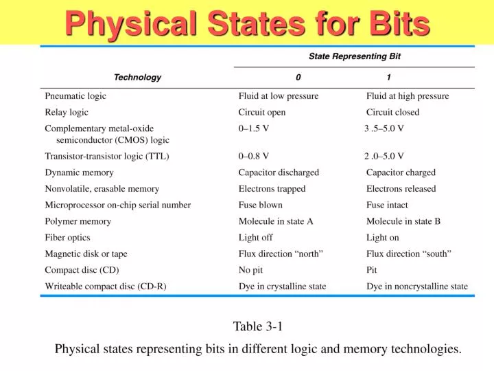
Physical States for Bits. Black Box Representations. Truth Tables. Basic Logic Gates. NAND and NOR gates. Sum of Products Circuits. Timing Diagrams. Logic Levels for CMOS. The concept of voltage-controlled resistance. nMOS transistor. pMOS transistor.

amos
Download Presentation

Physical States for Bits

An Image/Link below is provided (as is) to download presentation Download Policy: Content on the Website is provided to you AS IS for your information and personal use and may not be sold / licensed / shared on other websites without getting consent from its author. Content is provided to you AS IS for your information and personal use only. Download presentation by click this link. While downloading, if for some reason you are not able to download a presentation, the publisher may have deleted the file from their server. During download, if you can't get a presentation, the file might be deleted by the publisher.

E N D

Presentation Transcript


  1. Physical States for Bits

  2. Black Box Representations

  3. Truth Tables

  4. Basic Logic Gates

  5. NAND and NOR gates

  6. Sum of Products Circuits

  7. Timing Diagrams

  8. Logic Levels for CMOS

  9. The concept of voltage-controlled resistance

  10. nMOS transistor

  11. pMOS transistor

  12. Now we put together nMOS and pMOS transistors to create an inverter

  13. Switch Model for CMOS inverter

  14. Logical operation of CMOS inverter

  15. Explanation of 2-input CMOS NAND gate

  16. Switch Model for NAND realized in CMOS

  17. Explanation of CMOS NOR

  18. CMOS NAND with 3 inputs

  19. Example of realization of large NAND gates in CMOS

  20. Buffers realized in CMOS

  21. AND gate in CMOS

  22. AND-OR-INVERT gate in CMOS

  23. AND-OR-INVERT gate in CMOS

  24. CMOS OR-AND-INVERT

  25. CMOS OR-AND-INVERT

  26. Data Sheets and how to use them

  27. Test Circuits and Waveforms

  28. Input-Output Characteristics

  29. Logic Levels and Noise Margins for CMOS logic family

  30. Resistive Models of Inverters

  31. Resistive model for CMOS LOW output with resistive load

  32. Black Box Representations Resistive model for CMOS HIGH output with resistive load

  33. Circuit defintions to calculate currents

  34. Output loading specifications

  35. Estimating sink and source currents

  36. CMOS inverters with nonideal input voltages

  37. Black Box Representations CMOS inverter with load and nonideal 1.5 voltage input

  38. Black Box Representations CMOS inverter with load and nonideal 3.5 voltage input

  39. What to do with non-used inputs?

  40. Transition times

  41. How to analyze transition times for CMOS output?

  42. Model of HIGH-to-LOW transition

  43. Fall time

  44. Model of a CMOS Low-to-High Transition

  45. Rise time for a LOW-to-HIGH transition of a CMOS Output

  46. Propagation Delays for a CMOS inverter

  47. Worst-Case Timing using logic-level boundary points

  48. Ground bounce in an IC with eight inverters and one ground pin

  49. CMOS transition gate

  50. Two-input multiplexer using CMOS transmission gates

More Related