Download
1 / 49
490 likes | 676 Views
TCOM 503 Fiber Optic Networks. Spring, 2006 Thomas B. Fowler, Sc.D. Senior Principal Engineer Mitretek Systems. Topics for TCOM 503. Week 1: Overview of fiber optic communications Week 2: Brief discussion of physics behind fiber optics Week 3: Light sources for fiber optic networks

E N D
TCOM 503Fiber Optic Networks Spring, 2006 Thomas B. Fowler, Sc.D. Senior Principal Engineer Mitretek Systems
Topics for TCOM 503 • Week 1: Overview of fiber optic communications • Week 2: Brief discussion of physics behind fiber optics • Week 3: Light sources for fiber optic networks • Week 4: Fiber optic components fabrication and use • Week 5: Fiber optic components (continued); Modulation of light • Week 6: Optical fiber fabrication and testing of components • Week 7: Noise and detection
Useful web sites • A tutorial on testing optical systems: ftp://ftp.flukenetworks.com/public/cabling/DSP4000Series/DSP4000_CBT_2_1.EXE • A demo version of an optical network design program from RSOFT: http://www.rsoftdesign.com/products/evalform.cfm • Physics demos relevant to the course: http://www.colorado.edu/physics/2000/index.pl
Useful web sites (continued) • HP/Agilent material on bit error rate (BER) testing: http://we.home.agilent.com/cgi-bin/bvpub/agilent/reuse/cp_ReferenceRedirector.jsp?CONTENT_NAME=AGILENT_EDITORIAL&CONTENT_KEY=1000000386:epsg:apn&STRNID=03&LANGUAGE_CODE=eng&COUNTRY_CODE=ZZ
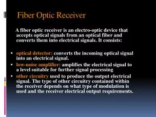
Noise and detection • Steps in signal reception and recovery • Contributors to signal degradation • Measure of performance: bit error rate • Ways of dealing with transmission problems
Basic problem • Maximize speed while keeping bit error rate (BER) low • BER is ultimate figure-of-merit for a given link of given speed • All other variables must be juggled to keep BER very low • Distance • Power • Coding • Fiber • Detector • Amplifiers
Typical system Source: Dutton
Steps in signal detection and recovery Bias control Automatic gain control PLL Bandpass filter l clock Detector (PIN or APD) Decoder Received bit stream Amplifier Pre-amplifier
Tasks of receiver • Decide where bits begin and end • Long strings of 0s or 1s may mean no light transitions for many bits • Decide what light amplitude represents a 0 and what represents a 1 • Involves a “decision point” which may be dynamic
The problem • Signal transmitted • Signal received
Steps in signal detection and recovery (continued) • Signal split into wavelengths • Each wavelength fed into receiver • Optical signal converted to electronic form using PIN or APD • Electronic signal amplified and filtered through bandpass filter to remove low and high frequency components • Further amplification of signal • Feedback loop stabilizes signal strength • Phase locked loop (PLL) used to recover timing • Timing used to determine when to make 0/1 decision • Bit stream fed into decoder (higher layer processing)
Limits to receiver performance • Reliable detection of a bit requires theoretical minimum of 21 photons • Real receivers require about 10x this amount • May be still higher if large amounts of noise present • Quantum efficiency of PIN diodes and other detectors goes down as speed increases • 10 Gbps ~ 0.8 • 20 Gbps ~ 0.65 • 40 Gbps ~ 0.33
Contributors to signal degradation • Noise • Jitter • Dispersion • Reflections • Scattering
Jitter • Difference between correct timing of a pulse and timing detected by receiver • Noise and distortion introduce slight timing errors • Vary at random • Causes • Nature of detection equipment • Smearing and distortion of pulses due to dispersion, action of filters and other components Source: www.ultranet.com
Noise • Random glitches in signal • Less of a problem in optical than in electrical circuits • Causes • Stray light • Imperfect components such as filters, switches • Light sources all have some noise • Amplifiers • Receiver circuitry
Dispersion • Smearing of pulses due to primarily to chromatic effects Source: Dutton
Reflections • Light transmitted backward due to imperfect components • Many devices use mirrors or rely on interference • Can reflect light if not perfect • Splices and connectors also are a source • Can occur at any junction between materials of different RI
Scattering • Light sent in random directions • Causes • Imperfections in fiber • SBS: diffraction caused by acoustic vibrations in fiber • Originates with electric field of light beam • SRS: diffraction caused by molecular vibrations in fiber • Originates with electric field of light beam
Signal (bit stream) recovery: PLL • Objective is to output a sine wave of same frequency and phase as input • This allows use of the output to “clock” the input pulses and determine when to read them in order to decide if 1 or 0 was transmitted
PLL (continued) • VCO produces clock frequency close to frequency being received • VCO output fed to comparison device which compares phase of input, VCO • Output of phase detector proportional to difference between input, VCO (error signal) • VCO adjusted to minimize error signal • Output taken from VCO
Decision problem • Given a certain observed photocurrent (or proportional voltage) received, which bit (0 or 1) is most likely to have been transmitted? • Probability question • Answer depends on average receiver response to transmission of 0 or 1 • Also depends on likelihood that 0 or 1 transmitted (so-called a priori knowledge) • Usually 50% in this case, but in multi-symbol environments can vary considerably • With this information a maximum likelihood algorithm can be generated
Decision problem (continued) • To get average response curves, create histogram • Send large number of 1s, record signal levels received • Divide into bins based on current received • Plot number received vs. current • Smooth out • Repeat for large number of 0s
Determining decision curve 25 20 Number in this range 15 10 5 4.0 5.0 3.0 4.5 5.5 2.0 2.5 .5 1.5 3.5 1.0 Photodetector current (ma)
Decision problem (continued) Area=fraction of time 0 will be decided when 1is correct Area=fraction of time 1 will be decided when 0is correct
Math background • Normal or Gaussian distribution: • Commonly referred to as N(m,s2) • Cumulative normal distribution, P(X), is integral of this from negative infinity to X
Math background (continued) • Complementary cumulative distribution function, Q(X), given by • It immediately follows that P(X) + Q(X) = 1
Math background (continued) • Pdf and cdf fornormal distri-bution Q(a)
Math background (continued) • Probability of value falling between a and b
Decision problem (continued) • If • s0 = variance of received photocurrent for 0 transmitted • s1 = variance of received photocurrent for 1 transmitted • I0 = mean value of received photocurrent for 0 transmitted • I1 = mean value of received photocurrent for 1 transmitted Then threshold photocurrent (decision point) Ith given by Ith = (s0 I1 + s1 I0)/(s0 + s1)
Decision problem (continued) • Can also be shown that bit error rate (BER) given by Q ((s0 I1 + s1 I0)/(s0 + s1)) where Q is the upper tail of Gaussian distribution • Smaller if argument larger • This can be shown to be approximately equal to Q((Imin2/(4NoB))1/2) where Imin = minimum signal amplitude B = bandwidth N0 = noise power
Decision problem (continued) • BER goes up if noise power increases Log of BER
Bit error rates (BER) • Early days (1970s) networks had error rates of 10-6 to 10-5 on slow copper links • Protocols designed to handle these high error rates • Nowadays layered protocols would choke on such rates • Single bit error could cause retransmission of up to 3000 cells • Acceptable rate today is 10-12 to 10-14
Tradeoffs in designing faster systems • Receiver sensitivity • Double speed requires doubling power at receiver (because it is received only half as long for each bit) • Higher sensitivity • Double power of transmitter • Shorten link by 15 km • Use multilevel coding
Tradeoffs in designing faster systems: Signal Bandwidth • Signal increases bandwidth of laser source by double the signal bandwidth • Modulating signal at 10 Gbps means increasing effective output bandwidth by 20 Gbps • At 1550 nm, 1.5 nm corresponds to about 125 GHz • Relevant formulae • For Gaussian pulse of time duration t0, spectral width sn = 1/pt0 • Bandwidth consumed by frequency range Df given by
Tradeoffs in designing faster systems: Signal Bandwidth where Df0 is center frequency, Dl0 is center wavelength, n is index of refraction (~1.5) • Dispersion problem • Doubling speed doubles dispersion • Doubling speed also halves pulse length, so same amount of dispersion has 2x effect • Net result is that doubling speed multiplies dispersion effects by 4 • 2.4 Gbps link 1000 km long can only be 65 km at 10 Gbps • Note that broad spectral range of LEDs precludes their use in long distance applications, as well as in applications where closely spaced wavelengths are needed
Tradeoffs in designing faster systems: nonlinear effects • Stimulated Brillouin Scattering (SBS) and Stimulated Raman Scattering (SRS) kick in at high powers • Large electric fields trigger vibrations in lattice which cause it to look like a diffraction grating • Incoming pulses are therefore scattered • Power threshold for SBS can be as low as 10 mW • Effectively imposes limit on maximum power that can be used to overcome noise and attenuation
System design • Electronics cost and complexity go up rapidly as speed increases • Theoretical limitations indicate that 10 Gbps may be practical limit for PCM systems • Scattering • Dispersion • 40 Gbps systems may appear • Note that 40 Gpbs corresponds to bandwidth of 80 GHz • 80 GHz requires about 1 nm, without guard bands • This is wider than ITU grid spacing
System design (continued) • More practical to increase speed in other ways • WDM • Multilevel codes • Solitons • Require optical time domain multiplexing
System parameters dependent on power • Signal-to-noise ratio (SNR) • Signal power/noise power • Can be improved up to a point by increasing laser power • Inter-symbol interference (ISI) • Merging of bits due to dispersion • Partially compensated with more power • Extinction ratio • If zero bit represented by power level > 0, then extinction ratio is power level of 1/power level of 0 • Low value can be compensated with more power
Determining how good a signal is as carrier of information • Classic measure is “eye diagram” • Made by superimposing large number of signal traces overtop of one another Source: Dutton
Eye diagram (continued) • Vertical opening ~ difference in signal level from 0 to 1 • Noise, other factors will reduce • Horizontal opening ~ amount of jitter • Large amount of jitter will reduce horizontal width • Thickness of bands at zero crossing also measure of jitter • Overall size of opening measure of how easy it is to correctly detect 1s and 0s • If eye is closed, nearly impossible to detect Source: Dutton
Eye diagram (continued) Source: Dutton
Eye diagrams (continued) 900 Mbps Cypress PSI system 2.5 Gbps Cypress PSI SONET system Source: Cypress Semiconductor
Eye diagrams (continued) Source: LeCroy
Eye diagram of VCSEL at 10 Gbps Source: IBM Micro News, Vol. 6, No. 2