Download
1 / 24
250 likes | 581 Views
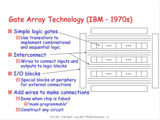
Gate array design. Use a sea of basic transistors (pmos/nmos) or gates (NAND/NOR) • Can have cells which can provide a universal logic function • Just need to add signal routing – only a few masks Advantages : • Reduced design time • Less chance of errors • Reduced production costs

E N D
Gate array design • Use a sea of basic transistors (pmos/nmos) or gates (NAND/NOR) • Can have cells which can provide a universal logic function • Just need to add signal routing – only a few masks Advantages: • Reduced design time • Less chance of errors • Reduced production costs • Decrease time to product DSD,USIT,GGSIPU
www.geocities.com/aps_ipu DSD,USIT,GGSIPU
Gate Array Design (Cont.) Disadvantages: • Very Limited flexibility • Need moderately high volume product • Less easily protected IPR DSD,USIT,GGSIPU
Programmable design • Use an array of logic cells • Cells can provide a universal logic function • Signal routing through switch box approach • RAM holds routing patterns (re-programmable) DSD,USIT,GGSIPU
Advantages: • Reduced design time • Easily reworked • Low design costs • Decrease time to product Disadvantages: • Limited flexibility • Low volume production • Less easily protected IPR DSD,USIT,GGSIPU
Programmable Logic Devices (PLDs) Programmable logic device, or PLD, is a general name for a digital integrated circuit • capable of being programmed to provide a variety of different logic functions. There are four main families of PLDs: - Programmable logic arrays (PLA) - Programmable array logic devices (PAL) - Read-only memories (ROM) - Complex PLDs (FPGAs, RAM) DSD,USIT,GGSIPU
Programmable switches allow connections to be made in an array of logic gates. We will look at the operation of each and examples of combinatorial and sequential design with each. DSD,USIT,GGSIPU
Programmable Logic Devices (PLDs) What are the advantages of programmable logic devices? • simple PLDs can realise from 2 to 10 functions of 4 to 16 variables on a • single integrated circuit • excellent for prototyping designs • it is possible to replace a number of SSI devices with a single device to • realise logic networks DSD,USIT,GGSIPU
single chip required to implement (possibly large) logic designs • complex PLDs can be used realise complex digital systems – even processors! • PLDs allow us to simplify designs and reduce development times – hence reduced overheads! • changes in the design can be easily implemented by reprogramming the device DSD,USIT,GGSIPU
Programmable Technology * Fusible link devices - e.g. the PROM - Blowing a fuse breaks a link between lines - Once programmable - Very high density possible * Electrical switching elements - e.g. the EPROM, EEPROM • nMOS transistors used to ‘switch’ connections between lines • Devices can be re-programmed • Relatively high density • How do we program PLDs? DSD,USIT,GGSIPU
Structure of PAL DSD,USIT,GGSIPU
Layout of a part of a Programmable Logic Cell DSD,USIT,GGSIPU
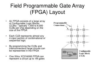
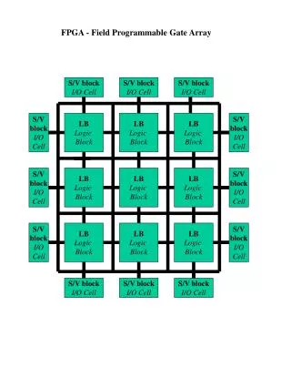
Structure of a FPGA DSD,USIT,GGSIPU
Configuration of Memory Cell DSD,USIT,GGSIPU
Configuration of Xilinx 300 DSD,USIT,GGSIPU
Programmable I/O DSD,USIT,GGSIPU
General Purpose Interconnect DSD,USIT,GGSIPU
Direct Interconnect DSD,USIT,GGSIPU
Vertical and Horizontal long line DSD,USIT,GGSIPU
EPROM Programmable Switches DSD,USIT,GGSIPU
Actel antifuse structure DSD,USIT,GGSIPU
Altera 700 Logic Array Blocks DSD,USIT,GGSIPU
Xilinx 7000 CLB DSD,USIT,GGSIPU
References • S. Brown, R. Francis, J. Rose, Z. Vranesic, Field-Programmable Gate Arrays, Kluwer Academic Publishers, May 1992. • S. Trimberger, Ed., Field-Programmable Gate Array Technology, Kluwer Academic Publishers, 1994. • J. Rose, A. El Gamal, A. Sangiovanni-Vincentelli, “Architecture of Field- Programmable Gate Arrays,” in Proceedings of the IEEE, Vol. 81, No. 7, July 1993, pp. 1013-1029. • J. Oldfield, R. Dorf, Field Programmable Gate Arrays, John Wiley & Sons, New York, 1995. • C.H.Roth, DSD with VHDL, Thomson Learning DSD,USIT,GGSIPU