Download
1 / 25
270 likes | 530 Views
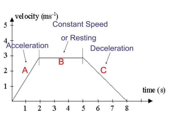
Carrier Mobility and Velocity. Mobility - the ease at which a carrier (electron or hole) moves in a semiconductor Symbol: m n for electrons and m p for holes Drift velocity – the speed at which a carrier moves in a crystal when an electric field is present

E N D
Carrier Mobility and Velocity • Mobility - the ease at which a carrier (electron or hole) moves in a semiconductor • Symbol: mn for electrons and mp for holes • Drift velocity – the speed at which a carrier moves in a crystal when an electric field is present • For electrons: vd = mn E • For holes: vd = mp E
Four Point Probe • Probe tips must make an Ohmic contact • Useful for Si • Not most compound semiconductors
Diffusion • When there are changes in the concentration of electrons and/or holes along a piece of semiconductor • the Coulombic repulsion of the carriers force the carriers to flow towards the region with a lower concentration.
Mobility vs. Dopant Concentration in Silicon http://www.ioffe.ru/SVA/NSM/Semicond/Si/electric.html#Hall
Van der Pauw • Four equidistant Ohmic contacts • Contacts are small in area • Current is injected across the diagonal • Voltage is measured across the other diagonal Top view of Van der Pauw sample http://www.eeel.nist.gov/812/meas.htm#geom
Calculation • Resistance is determined with and without a magnetic field applied perpendicular to the sample. F is a correction factor that takes into account the geometric shape of the sample.
Hall Measurement • See http://www.eeel.nist.gov/812/hall.html for a more complete explanation http://www.sp.phy.cam.ac.uk/SPWeb/research/QHE.html
Calculation • Measurement of resistance is made while a magnetic field is applied perpendicular to the surface of the Hall sample. • The force applied causes a build-up of carriers along the sidewall of the sample • The magnitude of this buildup is also a function of the mobility of the carriers where A is the cross-sectional area.
N vs. P doping The sign of the Hall voltage, VH, and on D R13,24 in the Van derPauw measurement provide information on doping.
Epitaxial Material Growth • Liquid Phase Epitaxy (LPE) • Vapor Phase Epitaxy (VPE) • Molecular Beam Epitaxy (MBE) • Atomic Layer Deposition (ALD) or Atomic Layer Epitaxy (ALE) • Metal Organic Chemical Vapor Deposition (MOCVD) or Organometallic Vapor Phase Epitaxy (OMVPE)
MBE • Wafer is moved into the chamber using a magnetically coupled transfer rod • Evaporation and sublimation of source material under ultralow pressure conditions (10-10 torr) • Shutters in front of evaporation ovens allow vapor to enter chamber, temperature of oven determines vapor pressure • Condensation of material on to a heated wafer • Heat allows the atoms to move to appropriate sites to form a crystal
Schematic View http://web.tiscali.it/decartes/phd_html/III-Vms-mbe.png
http://ssel-front.eecs.umich.edu/Projects/proj00630002.jpg http://www.mse.engin.umich.edu/research/facilities/132/photo
Advantages • Slow growth rates • In-situ monitoring of growth • Extremely easy to prevent introduction of impurities
Disadvantages • Slow growth rates • Difficult to evaporate/sublimate some materials and hard to prevent the evaporation/sublimation of others • Hard to scale up for multiple wafers • Expensive
MOCVD • Growths are performed at room pressure or low pressure (10 mtorr-100 torr) • Wafers may rotate or be placed at a slant to the direction of gas flow • Inductive heating (RF coil) or conductive heating • Reactants are gases carried by N2 or H2 into chamber • If original source was a liquid, the carrier gas is bubbled through it to pick up vapor • Flow rates determines ratio of gas at wafer surface
Schematic of MOCVD System http://nsr.mij.mrs.org/1/24/figure1.gif
http://www.semiconductor-today.com/news_items/2008/FEB/VEECOe450.jpghttp://www.semiconductor-today.com/news_items/2008/FEB/VEECOe450.jpg
Advantages • Less expensive to operate • Growth rates are fast • Gas sources are inexpensive • Easy to scale up to multiple wafers
Disadvantages • Gas sources pose a potential health and safety hazard • A number are pyrophoric and AsH3 and PH3 are highly toxic • Difficult to grow hyperabrupt layers • Residual gases in chamber • Higher background impurity concentrations in grown layers
Misfit Dislocations • Occur when the difference between the lattice constant of the substrate and the epitaxial layers is larger than the critical thickness. http://www.iue.tuwien.ac.at/phd/smirnov/node68.html
Critical Thickness, tC where b is the magnitude of the lattice distortion caused by a dislocation (Burger vector) f is the mismatch between the lattice constants of film and the substrate n is Poisson’s ratio (transverse strain divided by the axial strain).