Download

1 / 21
210 likes | 353 Views
Spike Sorting Algorithm Implemented on FPGA. Elad Ilan Asaf Gal Sup: Alex Zviaginstev. Goals & Targets. Implement a detect & sort algorithm of Neural spike on FPGA. Explore different algorithmic options and implementations for better performance. The general system. Requirements.

E N D
Spike Sorting Algorithm Implemented on FPGA Elad Ilan Asaf Gal Sup: Alex Zviaginstev
Goals & Targets • Implement a detect & sort algorithm of Neural spike on FPGA. • Explore different algorithmic options and implementations for better performance.
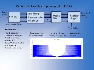
Requirements • Low frequency: ~100KHz input rate. • Small H/W as possible • Very low power consumption • Low output rate as possible
Algorithm overview • Learning phase: • Apply PCA algorithm on a set of learning data • Extract best separation lines from the learning data. • Store separation lines parameters in chip registers.
Algorithm overview • Real time sorting: • Apply threshold detection to raw data • Calculate speculative projections on PC space, for a set of predefined alignments. • Find the most suitable alignment (maximum find) • Sort the spike by comparing to separation lines
Operation modes • LDPC mode: In this mode PC data is loaded into internal registers. The data is input on the SPKDATA pin, and the PC index is set by PCSEL pin (‘0’ – PC1, ‘1’ – PC2). The registers depth is the same as the spike length. • WRCR mode: In this mode the unit updates the control register with address on pin CRADDR with the value on pin CRDATA. • RDCR mode: In this mode the value in the CR with address on pin CRADD is written to output pin CRDATAOUT • SORT mode: In this mode unit sorts the spike data on pin SPKDATA. • IDLE mode: In this mode no operation is done in the unit. CR values are kept. • RST
Implementation • Block diagram:
Implementation • Detection block:
Implementation • Extraction block:
Implementation • Sorting block:
Implementation • Control block:
Implementation • Pipeline diagram
Implementation • Pipeline diagram
H/W characterization • 100KHz input rate 20MHz internal clock freq. • 40 input data pins • 27 output pins • W/C output rate: 500Hz x 19 pins • # of logic gates: ??? • # of seq. elements: ~5K
HDL code written Only partly validated. Environment almost ready (for HDL model) Current status
Future time line • Till end of Jan: • Validation finished • First simulation • Initial syn runs • Initial P&R • H/W order • Validation finished • February – Asaf in RD