Download
1 / 18
180 likes | 306 Views
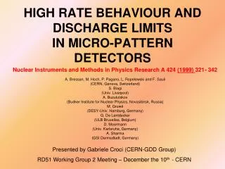
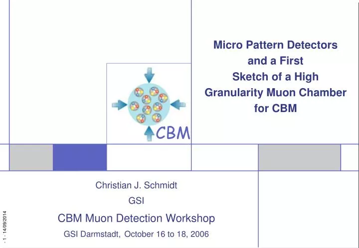
Micro Pattern Detectors and a First Sketch of a High Granularity Muon Chamber for CBM. Christian J. Schmidt GSI CBM Muon Detection Workshop GSI Darmstadt, October 16 to 18, 2006. Outline. History of micro pattern detectors The GEM in particular Sketch of a GEM-based Muon chamber.

E N D
Micro Pattern Detectorsand a FirstSketch of a High Granularity Muon Chamber for CBM Christian J. Schmidt GSI CBM Muon Detection WorkshopGSI Darmstadt,October 16 to 18, 2006
Outline • History of micro pattern detectors • The GEM in particular • Sketch of a GEM-based Muon chamber
Micro-Pattern Gas Detectors: many similar concepts Very creative phase in the ninties: seeking advances beyond the MWPC for targeted HEP-experiments MSGC by Anton Oed (first µ-detector concept originated in neutron physics) GEM by Fabio Sauli MICROMEGAS by Y. Giomataris and G. Charpak et al. Micro-DOT by Biagi µCAT (Compteur a trous) by Lemonnier ... Micro Wire, Micro-Pin Array (MIPA), Micro-Tube ... ... Micro-Well, Micro-Trench, Micro-Groove ... most importantly: micro = fast due to short ion drift Overview: F. Sauli and A. Sharma: Micropattern Gaseous Detectors, Ann. Rev. Nucl. Part. Sci. 49(1999)341
The Gas Electron Multiplier (GEM) Electrons Ions Amplifier Mode • In hole high fields allow Gas amplification 1 - 400 pictures from Sauli Transparent Mode • At gain 1, electric fields transport charges through the holes
GEM- History since invention 1997 by F. Sauli • HERA-B: First HEP-Experiment to push from kHz to MHz event-rate • First HEP-Experiment to employ MSGCs on large scale • - Detect minimaly ionizing particles (tracks) in inner tracker • detector, depositing approx. 1 to 10 keV • - But get highly ionizing events up to 50000 times stronger also • rapid ageing • direct discharge damage to microstructures • - GEM was to introduce two step charge amplification, • leaving MSGC-amplification at a moderate gain of 50 to 300. damage at MSGC HERA-B inner tracker module, an MSGC-GEM combination 200 built at Heidelberg 50 my development effort by Eisele et al.
GEM- History COMPASS @ CERN: Large scale employment of tripple GEM tracking detectors 31cm x 31cm (operative!) Today, HEP have largely decided for Si-Strip-Detectors: CMS LHCB ALICE ... GEMs not robust enough for signal spectrum with MIPs and HIPs Silicon strip detectors are industrially availability today (Hamamatsu) HEP application left: TPC – at Linerar Colliders etc. (TESLA)
Other current and some exotic applications for GEMs • Single photon detection employing mutiple, cascaded GEMs Breskin et al., C. Richter (Diss.) • Gain and readout for TPCs in HEP (M. Killenberg et al.) • Coherent Neutrino Detection (J. Collar et al. 2003) • low background materials • sensitivity to sub keV recoil energies • feasibility of very high gain (~105) at very high pressure (20 atm) • Solid converter neutron detection (CASCADE-Detector) • Optical readout of scintillation after neutron conversion through 3He Fraga et al., G. Manzin (ILL) • GEM-preamp for Ultra Cold Neutron detection (Heidelberg) • X-Ray Polarimeter (E. Costa et al., R. Bellazini et al.)
Particular, unique properties of GEMs • allow multi-stage amplification • amplification decoupled from readout • avoid high gain photon positive feedback • single photon detection with suppression of ion- as well as photon-feedback • inherent high rates capability through micro scale • minimal magnetic distortion through micro scale • robust technology • “simple” lithographic production process industrially available • production by CERN and in the future by Polish CERN licencee ... ??? • 3M has also developed a large scale production process for 12´´ x 12´´
Multiple GEM structures high gain - - high breakdown limit S. Bachmann et al, Nucl. Instr. and Meth. A479 (2002) 294
GEM high rates capability FAST ELECTRON SIGNAL (NO ION TAIL) The total length of the detected signal corresponds to the electron drift time in the induction gap: Full Width 20 ns (for 2 mm gap) taken from Sauli et al.: http://www.cern.ch/GDD
GEM high rates capability > 105 Hz/mm2 taken from Sauli et al.: http://www.cern.ch/GDD
Towards a Micropatterned Muon Chamber Model a Readout System • In contrast to Silicon, gas detectors allow for gain (fudge factor) • As learned yesterday, we expect to get at maximum (close to the axis) 1 Track/cm2/event with a 1 MHz event rate. too much for wire chambers but comfortable for micro pattern detectors such as GEMs (limit beyond 10 MHz/ cm2) • Mostly MIPs, but should expect all kinds of garbage (e.g. neutrons)! • First Muon chamber measures about 2m in diameter, A~3m2 Is it feasible to step from Silicon strips in the STS to a micro patterned gas detector as first Muon chamber... ... employing the same readout front-end ?
Have a look at a Silicon Strip Detector • Sensor thickness ~ 250 to 300 µ • Sensor pitch 50.7 µ • Gap 32.7 µ Manufacturer quotes 1.5 pF/cm strip length e = 11.8 The average strip length will be about 10 to 15 cm, giving 15 to 22.5 pF strip capacitance - central sensors have shorter strips, longer cables - outer sensors have longer strips, shorter cables - strip area about 5 mm2
Model Sensor to Scale Capacitance • Purely 2D electrostatic problem, 2D Poisson solvers available, also some analytical solutions • Capacitance scales with ratios of characteristic geometric lengths: strip-gap/strip-width, strip-width/sensor-thickness • Model Silicon strip as a strip-line: get C = 1.23 pF/cm • sensor thickness non essential, lower electrode may be abolished • Strip impedance 69 Ohm, signal phase velocity 0.4 c, effective e = 6.5 • Capacitance scales with effective e as1/e e
Gas Detector Scaled from Silicon • With identical, scalable geometry, e = 1 or 1.1 get C = 190 fF/cm • Scale readout by a factor of 10 and get the same capacitance: • Strip pitch 0.5 mm, sensor thickness 2 - 3 mm • Gems at 2 to 3 mm distance have no influence on capacitance • Strip impedance 175 to 200 Ohm • Strip width of 180 µ comfortably realizable Feasible strip length for silicon readout electronics: 65 cm e
Corresponding Detector Strip Area • 65 cm of 0.5 mm strip pitch corresponds to 3.25 cm2 • Central region needs higher granularity, up by a factor of about 10 in order to avoid hit pile-up. • Cap. = 1.2 pF, so 10 pF may be spend on cabling, A = 0.33 cm2 • Lateral regions have little rate, so may be operated with higher strip areas. • What is the necessary resolution? Here we need some input from the tracking side!
Proposal for a CBM First Muon Chamber • MIPs: dE/dx for Argon at normal pressure 2.7 keV/cm, giving 90 e-ion pairs per cm. • For Silicon sensors, a MIP gives about 50 000 e-hole pairs. • Parallax and local tacklet tracking may demand for higher granularity in drift-time detection, resulting in 1 mm drift resolution. Q = 9 e-/mm • need quite some gain for detection two GEM layers to guarantee gain of 1000 to 10 000. Drift Drift Region GEM 2 GEM 1 RO Strips Signal channeling electrode
Conclusion • A GEM gas chamber appears to be a suited solution for the first Muon chamber. GEMs nicely match the specified rate capability of 106 Hz/cm2. • Detector capacitance may be chosen to perfectly adapt to Silicon optimized readout electronics. • The Gas detector wins with a factor of 6.5 effective e over Silicon, allowing for much longer structures (longer by the same factor of 6.5). • Lack of signal intensity needs to be compensated for by gain • The double GEM layer allows for gain up to 10 000 with limited sparking probability.