Download
1 / 1
10 likes | 149 Views
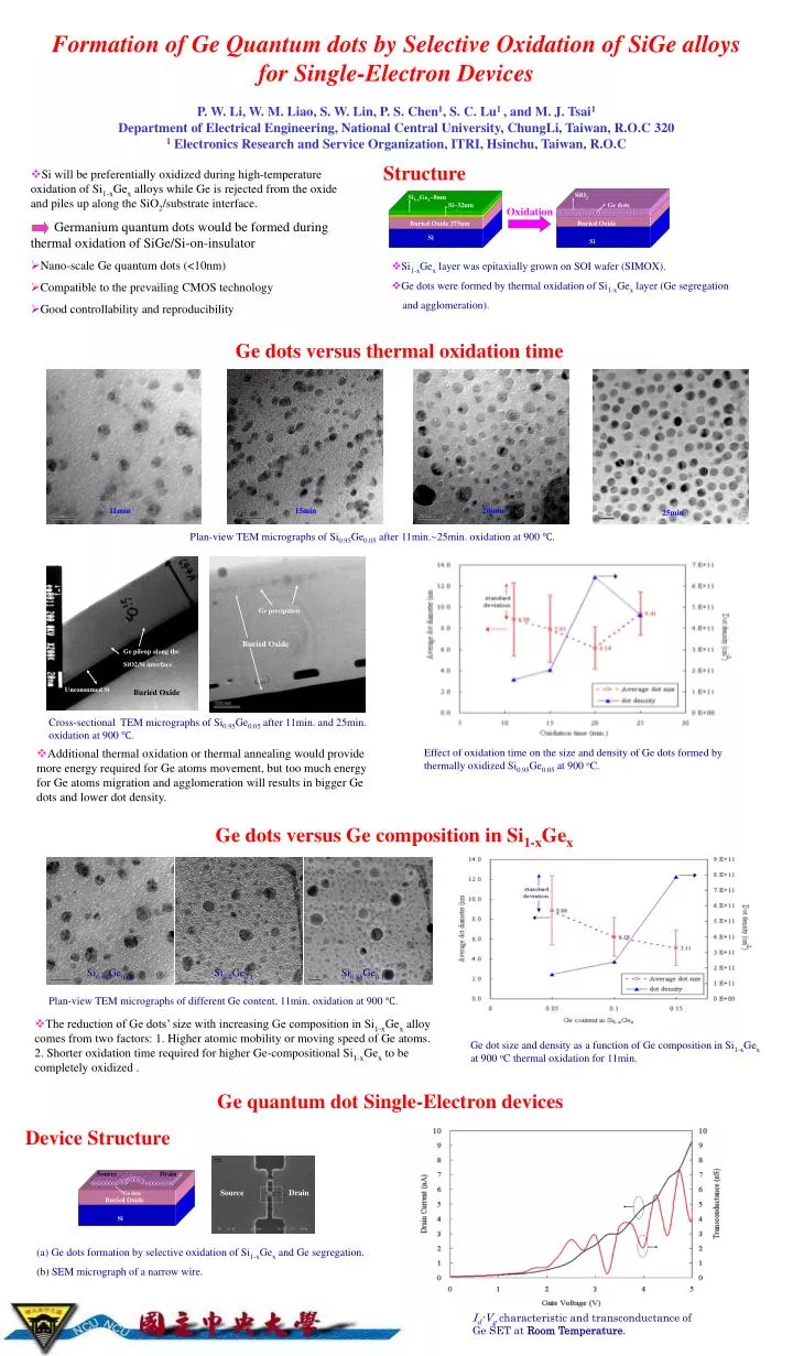
11min. 15min. 20min. 25min. Ge pileup along the SiO2/Si interface. Unconsumed Si. Buried Oxide. Formation of Ge Quantum dots by Selective Oxidation of SiGe alloys for Single-Electron Devices P. W. Li, W. M. Liao, S. W. Lin, P. S. Chen 1 , S. C. Lu 1 , and M. J. Tsai 1

E N D
11min 15min 20min 25min Ge pileup along the SiO2/Si interface Unconsumed Si Buried Oxide Formation of Ge Quantum dots by Selective Oxidation of SiGe alloys for Single-Electron Devices P. W. Li, W. M. Liao, S. W. Lin, P. S. Chen1, S. C. Lu1 , and M. J. Tsai1 Department of Electrical Engineering, National Central University, ChungLi, Taiwan, R.O.C 320 1 Electronics Research and Service Organization, ITRI, Hsinchu, Taiwan, R.O.C Structure • Si will be preferentially oxidized during high-temperature oxidation of Si1-xGex alloys while Ge is rejected from the oxide and piles up along the SiO2/substrate interface. Germanium quantum dots would be formed during thermal oxidation of SiGe/Si-on-insulator • Nano-scale Ge quantum dots (<10nm) • Compatible to the prevailing CMOS technology • Good controllability and reproducibility SiO2 Si1-xGex~8nm Si~32nm Ge dots Oxidation Buried Oxide 375nm Buried Oxide Si Si • Si1-xGex layer was epitaxially grown on SOI wafer (SIMOX). • Ge dots were formed by thermal oxidation of Si1-xGex layer (Ge segregation and agglomeration). Ge dots versus thermal oxidation time Plan-view TEM micrographs of Si0.95Ge0.05 after 11min.~25min. oxidation at 900 ℃. Ge precipition Buried Oxide Cross-sectional TEM micrographs of Si0.95Ge0.05 after 11min. and 25min. oxidation at 900 ℃. • Additional thermal oxidation or thermal annealing would provide more energy required for Ge atoms movement, but too much energy for Ge atoms migration and agglomeration will results in bigger Ge dots and lower dot density. Effect of oxidation time on the size and density of Ge dots formed by thermally oxidized Si0.95Ge0.05 at 900 oC. Ge dots versus Ge composition in Si1-xGex Si0.95Ge0.05 Si0.9Ge0.1 Si0.85Ge0.15 Plan-view TEM micrographs of different Ge content, 11min. oxidation at 900 ℃. • The reduction of Ge dots’ size with increasing Ge composition in Si1-xGex alloy comes from two factors: 1. Higher atomic mobility or moving speed of Ge atoms. 2. Shorter oxidation time required for higher Ge-compositional Si1-xGex to be completely oxidized . Ge dot size and density as a function of Ge composition in Si1-xGex at 900 oC thermal oxidation for 11min. Ge quantum dot Single-Electron devices Device Structure Source Drain Source Drain Ge dots Buried Oxide Si (a) Ge dots formation by selective oxidation of Si1-xGex and Ge segregation. (b) SEM micrograph of a narrow wire. Id-Vg characteristic and transconductance of Ge SET at Room Temperature.