Download
1 / 2
20 likes | 150 Views
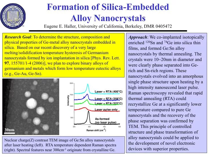
Laser + RTA (400°C). Laser + RTA (359°C). Laser + RTA (323°C). Laser pulse only. As-formed (no laser pulse). 30nm. Formation of Silica-Embedded Alloy Nanocrystals Eugene E. Haller, University of California, Berkeley, DMR 0405472.

E N D
Laser + RTA (400°C) Laser + RTA (359°C) Laser + RTA (323°C) Laser pulse only As-formed (no laser pulse) 30nm Formation of Silica-EmbeddedAlloy NanocrystalsEugene E. Haller, University of California, Berkeley, DMR 0405472 Approach: We co-implanted isotopically enriched 120Sn and74Ge into silica thin films, and formed Ge:Sn alloy nanocrystals by thermal annealing. The crystals were 10~20nm in diameter and were clearly phase separated into Ge-rich and Sn-rich regions. These nanocrystals evolved into an amorphous single phase structure upon heating by a high intensity nanosecond laser pulse. Raman spectroscopy revealed that rapid thermal annealing (RTA) could recrystallize Ge at a significantly lower temperature compared to pure Ge nanocrystals and the recovery of the phase separation was confirmed by TEM. This principle of controlled structure and phase transformation of alloy nanocrystals could be applied to the development of novel electronic devices with superior properties. Research Goal: To determine the structure, composition and physical properties of Ge-metal alloy nanocrystals embedded in silica. Based on our recent discovery of a very large melting/solidification temperature hysteresis of Germanium nanocrystals formed by ion implantation in silica [Phys. Rev. Lett. 97, 155701/1-4 (2006)], we plan to explore binary alloys of germanium and metals which form low temperature eutectic alloys (e.g., Ge-Au, Ge-Sn). 20nm 20nm Nuclear charge(Z) contrast TEM image of Ge:Sn alloy nanocrystals after laser heating (left). RTA temperature dependent Raman spectra (right). Spectral features near 300cm-1 originate from crystalline Ge.
Formation of Silica-EmbeddedAlloy NanocrystalsEugene E. Haller, University of California, Berkeley, DMR 0405472 Education: Three graduate students (Swanee Shin, Christopher Liao, and Julian Guzman) have contributed to this project at the University of California at Berkeley. S. Shin and C. Liao have continued nanocrystal research and have improved their synthesis, processing, and characterization skills. J. Guzman has joined the project andand he also performs research on optical properties of Erbium and Ge doped silica. Phase change memory cell (courtesy IBM Almaden research lab) Broader Impact: Flash memory is currently widely used for data storage in electronic devices, including digital cameras, cellular phones, personal computers, etc. As the size of individual storage cells approaches the scaling limit of the current technology, new types of memories based on phase change materials (PCMs) are emerging as promising potential replacements. Since PCMs based memory utilizes a thermal process to control the phase dependent electronic properties, alloy nanocrystals could be good candidates for PCM and other devices, once we can control reproducibly the temperature dependent phase and its electronic properties.