Download
1 / 10
100 likes | 110 Views
EXAMPLES OF FEEDBACK. Today we will Look at an example of negative feedback: a single transistor circuit with source resistance Look at an example of positive feedback: Schmitt trigger. NEGATIVE AND POSITIVE FEEDBACK.

E N D
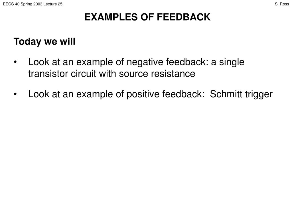
EXAMPLES OF FEEDBACK • Today we will • Look at an example of negative feedback: a single transistor circuit with source resistance • Look at an example of positive feedback: Schmitt trigger
NEGATIVE AND POSITIVE FEEDBACK A circuit exhibits feedback when the circuit input is affected by the value of the circuit output. Suppose some disturbance occurs in a circuit, changing the value of the output. If the circuit has negative feedback, the change in output adjusts the value of the input so as to bring the circuit back closer to its original state. If the circuit has positive feedback, the change in output adjusts the value of the input so as to make an even bigger change in the output. This continues until the circuit reaches a new stable state.
EXAMPLE OF NEGATIVE FEEDBACK Consider our usual transistor circuit, being used as a constant current source supplying the resistor RD. Problem: The transistor curves are greatly affected by changes in temperature. The relatively constant IDSAT supplied to RD increases as the circuit operates and heats up. This makes the current supplied by this constant current source unpredictable. Increased IDSAT could put the transistor in triode mode. VDD R1 RD R2
EXAMPLE OF NEGATIVE FEEDBACK When temperature rises, electron mobility m increases (generally). So, the ID vs. VDS curves get higher with heat. ID VGS = 3V, T = 150° VGS = 3V, T = 50° VGS = 2V, T = 150° VGS = 2V, T = 50° VDS
EXAMPLE OF NEGATIVE FEEDBACK Solution: Add a feedback resistor RS. VDD If ID increases (e. g. due to heat), VGS decreases. ID R1 RD This brings ID back down a little. + VGS - Small adjustments continue until an equilibrium is reached. R2 RS The final value of ID will be closer to the original “cold” value than it would be without feedback.
POSITIVE FEEDBACK: SCHMITT TRIGGER We used a comparator to “sharpen” a signal; to convert input voltages to either logic 1 (high rail) or logic 0 (low rail) depending on whether input is higher or lower than threshold. What if the signal had a high-frequency noise component? VIN VOUT Noise goes above and below 2.5 V rapidly… …causes VOUT fluctuation 2.5 V t t
POSITIVE FEEDBACK: SCHMITT TRIGGER A Schmitt trigger has a higher low-to-high threshold than high-to-low: VOUT VIN Now consider that noisy signal, sharpened with Schmitt trigger: VIN VOUT low-to-high threshold switches low to high, but not back to low since threshold far away high-to-low threshold Reduces fluctuations.
SCHMITT TRIGGER CIRCUIT “weak” inverter (larger VTH, lower ID-VDS curves) middle transistors have higher threshold magnitude, shallower ID vs VDS curves
SCHMITT TRIGGER CIRCUIT Low-to-high transition: middle NMOS remains cutoff even when left NMOS turns on Left NMOS takes current of both left PMOS and middle PMOS Left NMOS ID is higher than in normal unloaded inverter (for given VIN) Left NMOS VDS is higher than in normal unloaded inverter (for given VIN) VDS remains higher longer transitions later
SCHMITT TRIGGER CIRCUIT Now we reach the VIN value that turns on the middle NMOS… Now middle NMOS can accept current; less current remains for left NMOS. ID in left NMOS decreases. VDS on left NMOS decreases. VOUT, the inverse of VDS, increases. VGS on middle NMOS increases. ID in middle NMOS increases. ID in left NMOS decreases. Chain reaction causes rapid transition. The transition region is unstable. When we start up, we are pushed up all the way by positive feedback!