Download
1 / 22
220 likes | 579 Views
K. Makris 1 , D. Fragopoulos 1 , G. Tsiligiannis 1 , T. Lambaounas 1 , P. Anagnostopoulos 1 , C. Papadas 1 , J.P. Schoellkopf 2 , B. Glass 3 (1) Integrated Systems Development (ISD S.A.), Athens, GREECE (2) Advanced System Technology and User Service (ASTUS S.A.), Grenoble, FRANCE

E N D
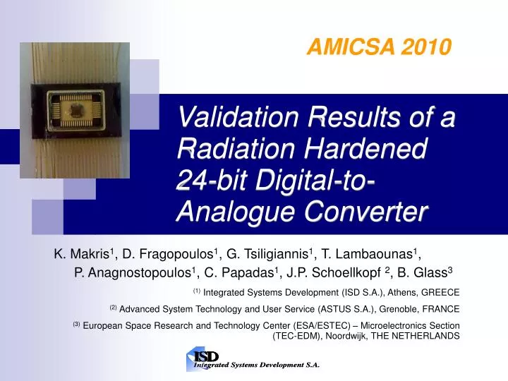
K. Makris1, D. Fragopoulos1, G. Tsiligiannis1, T. Lambaounas1, P. Anagnostopoulos1, C. Papadas1, J.P. Schoellkopf 2, B. Glass3 (1) Integrated Systems Development (ISD S.A.), Athens, GREECE (2) Advanced System Technology and User Service (ASTUS S.A.), Grenoble, FRANCE (3) European Space Research and Technology Center (ESA/ESTEC) – Microelectronics Section (TEC-EDM), Noordwijk, THE NETHERLANDS AMICSA 2010 Validation Results of a Radiation Hardened 24-bit Digital-to-Analogue Converter
Overview • Features • Architecture • Digital part • Analog part • Layout – chip fabrication • Package • Validation plan overview • Validation board and test setup • Electrical test results • Static performance summary • Dynamic performance summary • Radiation tests and setup • Radiation test results • Conclusions and future work
Product highlights • Features • Architecture: multi-bit ΣΔ modulator • Output stage: differential current steering • Digital input interface: Synchronous serial data format • Bandwidth: 0.1mHz – 1kHz • Sampling frequency: selectable 6kHz or 12 kHz • Oversampling ratio: selectable x256 or x128 • Configuration via I2C interface • 1.2V digital power supply • 3.3V analog power supply • Radiation tolerant design • Operating modes • Normal • Bypass • Test • Power down 1 Digital ON / Current sources OFF / Reference block ON • Power down 2 Digital ON / Current sources OFF / Reference block OFF • Applications • High accuracy instrumentation and actuator drive for systems operating in space
DAC24BISDA 1.2V 3.3V OUTP1 DAC 1 (Main) Interpolation stage Input interface SDIN SCLK OUTM1 SYNC I2C interface SDA Ref. Voltage 3rd order ΣΔ modulator Reference block SCL Level Shifters (1.2 - 3.3V) Clock Distribution network OUTP2 MCLK DWA DAC 2 (Redundant) OUTM2 Test signals DFT System Overview
Clock Distribution network 1.2V MCLK Digitalinput interface SDIN IRP1Linear Phase X2 IRP2Halfband X2 IRP3Halfband X2 SINCX32/X16 DATAp1 [31:0] SCLK SYNC DATAm1 [31:0] Interpolator CLK1 I2C Registers bank PDN_ANA Digital to Analog interface block (Level Shifters) 3rd order ΣΔ Modulator Write Read I2C interface SDA DATAp2 [31:0] DATAm2 [31:0] SCL DFT block CLK2 DWA Test signals DATA [31:0] Architecture: Digital Part (1/2)
Architecture: Digital part (2/2) • Modulator design • 3rd order feed-forward ΣΔ modulator • 5-bit quantizer • Sampling frequency 6kHz when OSR X256 and 12kHz when OSR X128 • Idle Tone avoidance by introduction of dither • Dynamic Element Matching (DEM) • The output element mismatch error is minimized by the use of a DEM algorithm. • Data Weighted Averaging (DWA) as an efficient DEM algorithm. • Algorithm's objective → achieve an equal use of elements in long-term by rotating the output elements (current sources) in a cyclic fashion. • DWA uses only one index, which is updated with the addition of the input every clock cycle.
Architecture: Analog Part • Bandgap cell provides an accurate reference voltage (1.2V) with a low temperature coefficient. • First order RC filter reduces any noise from the bandgap block. • Low noise Op-Amp along with M1 and current setting resistor (Rref or Rext) implements the reference current source for generating the reference current Iref. • IRef can be set by selecting the internal resistor RRef or connecting an external resistor Rext. • Differential elementary current sources built around the regulated cascode topology. • Use of PMOS transistors for lower flicker noise(1/f) and high linearity.
Radiation hardening techniques • Technology level:ST Microelectronics HCMOS9 0.13 um is a rad-hard proven technology. • Library level: For the digital part the most oversized and robust standard cells were used (including latches and flip-flops). • Digital design level • Fault masking by TMR (e.g. FSMs) • Synchronous reset • Reset assertion in the SINC block every 32 clock cycles • Analogue design level • Current source transistors with increased W/L ratio for increased capacitance and driving power. • Layout level • Deep N-well isolation (NISO): The entire digital part and all the NMOS devices of the analogue part are placed inside a deep n-well to minimize digital feed-through and latch-up susceptibility (see slide 10). • P+ guard rings surround the n-channel devices to cut any possible radiation induced parasitic paths. • Increased distance between the p+ diffusion in the well and the n+ in the substrate. • Increased number of substrate and well contacts.
Polarization block Current sources matrix Analog ring 1840 um 1840 um Digital ring Digital core Floor-plan and fabricationhighlights • Technology: 0.13um HCMOS9-GP ST-MicroelectronicsTM6 metal layers • Line name: DAC24BISDA • Dimensions: ~ 1840 x 1840 um • Total area: 3.42mm2 • No of I/O pads: 43 • Minimum pad-to-pad spacing: 90um 48-lead hermetically sealed ceramic flat package
Process • Deep N-Well isolation (NISO) • Minimizes the digital feed-through to the sensitive analog nodes • Improves the latch-up immunity • Layout and polarization scheme:
Package • 48 lead hermetically sealed ceramic flat package • Well proven space reliability (ST products) • External dimensions: (E1 x D) 9.65 x 15.72mm • Die attach cavity dimensions: (L x W) 5.58 x 3.55mm • Bonding pad cavity dimensions: (L x W) 8.50 x 5.46
Validation plan overview • Functional and performance validation - characterization • Static performance tests • INL, DNL • Offset and gain errors • Power consumption • Output current levels • Dynamic performance tests • THD+N • SNR, ENOB • Dynamic range • Radiation sensitivity tests • SEE → SEU, SEL • TID DAC24BISDA validation Functional Performance Device Characterization Radiation tests
Validation board System block diagram • Modular architecture --> Motherboard + DUT daughterboard • FPGA based design • Memories • UART and USART interfaces • Dedicated power supplies for the DUT • On-board ADC and footprint for a secondDAC for performing the SEU tests. FLASH memory DUT Power Supply domains DAC Outputs (SMA) ADC Remote keypad DAC DUT
Validation results: Test conditions • Unless otherwise noted, the following test conditions apply for all the tests: • Minimum: Digital power supplies VD=1.08V and analog power supplies VA=3.0V • Typical: VD=1.2V and VA=3.3V • Maximum: VD=1.25V and VA=3.6V • Ambient temperature: Ta=25ºC • Internal reference current setting resistor Rref=219 Ω • fMCLK=1.536 MHz • OSR x 256 (fs=6 kHz) • Output load: resistive 100 Ω (1% tol.) // 300 pF ceramic capacitor.
Static electrical parameters summary (*) It is possible to reduce the analog power consumption by using a higher external current setting resistor Rext.
Time domain waveform • Differential output DAC1, normal mode, sine wave 100Hz -1dBFS
Dynamic electrical parameter summary • Results • Dynamic range (DR): 113 dB • THD+N (SINAD): 108dB • Normal Mode, sine 100 Hz / -3 dBFS, MBW=1kHz, unbalanced output 110 dB ‘bulge’ due to insufficient data
Radiation tests • Preliminary radiation tests include TID and SEE (SEU, SEL) • Up to now only TID testing has been performed • TID test location: Co-60 source at ESA-ESTEC, The Netherlands • Dose rate setting by adjusting the distance between the DUT and the source (X) TID test setup overview X C0-60 facility at ESA-ESTEC
Radiation test results summary • TID testing • DUT sample setup • Under bias conditions • Constant sourcing of maximum output current (both DAC ON) • Monitored parameters • OUTP1, OUTM1, OUTP2, OUTM2, VPOL, VBGOUT, IA, ID • Radiation parameters • Constant dose rate: 85.4 Rad/min • Total accumulated dose: 111.4 kRad (H20) approx. 100 kRad (Si) • Data recording sampling rate: 1 measurement / min • Results • No change in the value of the monitored parameters through the duration of the test. • No abnormal operation observed
Conclusions and future work • The cut 2.0 has been released in order to: • include some enhancements in the digital part (serial input interface, register triplication) • deduce derivatives (100Ksamples and 1 Msamples) • Perform a detailed SEU and SEL analysis • The part is included in the catalog of ST-Microelectronics for space application products • Qualification for use in space will follow.
Thank you for your attention! Questions?