Download
1 / 12
190 likes | 561 Views
ME-250 Precision Machine Design Semiconductor Lithography Tool. Alok Bhatt Sarang Deshpande Instructor: Dr. B. J. Furman Mechanical and Aerospace Engineering Department San Jose State University Fall 2004 21 st Oct 2004. Overview. Traditional lithography tool

E N D
ME-250 Precision Machine Design Semiconductor Lithography Tool Alok Bhatt Sarang Deshpande Instructor: Dr. B. J. Furman Mechanical and Aerospace Engineering Department San Jose State University Fall 2004 21st Oct 2004
Overview • Traditional lithography tool • Precision aspects involved • Concept of HTM • Moving interferometer wafer stage • Precision aspects involved • Precision concepts in interference lithography • References ME-250 Fall 2004
Schematic of Photolithography Tool ___________________________________________________________________________________________________________ Source: www.binnard.com/SJSUlitho.ppt ME-250 Fall 2004
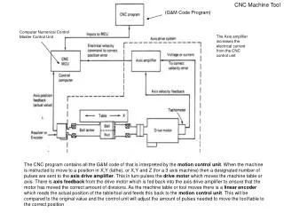
Schematic Diagram of Photolithography Tool Components of the lithography tool 10 – Linear Motor 66 – Wafer Table 68 – Wafer 72 – Metrology Frame 74 – Illumination Assembly 76 – Reticle 78 – Lens 80 – Photomask 102 – Wafer Stage Base 104 – Wafer Table 106 – Flexures 112 - Encoders 122 – Vibration Isolators 124 – Vibration Isolators 126 – Air Bearings 201 – AF/AL Emitter 202 – AF/AL Receiver 203 – Voice coil Motor z Reticle Stage x Y Lens Linear Motor 2X Wafer Stage VoicecoilMotor 2X _________________________________________________________________________________________________________________ Source: www.uspto.gov (US Patent # 6,686,991) ME-250 Fall 2004
Precision Engineering Principles Involved • Two linear motors provide motion to wafer stage in Y-axis. Plurality of motors eliminates Abbe Error • Three voice coil motors for positioning the wafer table relative to wafer stage in Z-axis • Two flexures to restrict the planner motion of the wafer table in X and Y axis, while allowing its motion in Z-direction • Vibration isolators to resist the vibrations to transfer from base to wafer stage • Air bearings are used between wafer stage and wafer base. A thinner layer of pressurized air is applied while vacuum holds the stage in position • AF/AL (Auto Focus/ Auto Level) sensors provide the position of exposure point relative to the wafer • Plurality of encoders (112) determines the position of wafer table relative to wafer stage Flexures Encoders AirBearings VibrationIsolators ___________________________________________________________________________________________________________ Source: www.uspto.gov (US Patent # 6,686,991) ME-250 Fall 2004
Concept of HTM Utilized In Positioning of Wafer Stage • “r” are position vectors • “R” are the coordinate rotations • Coordinate Frame “O” is reference coordinate system • “O1” is coordinate frame for wafer stage • “O2” is coordinate frame for wafer stage base • “O3” is coordinate frame for wafer table • “O4” is coordinate frame for lens • Six different encoders determine position of each coordinate system and put them into a matrix form • Position of each coordinate system relative to the reference coordinate system is then determined by homogeneous transformation matrices (HTM) ______________________________________________________________________________________________________________________ Source: www.uspto.gov (US Patent # 6,686,991) ME-250 Fall 2004
Moving Interferometer Wafer Stage (Vertically Mounted) Components of the wafer stage assembly 10 – Wafer Stage 11 – Right handed Cartesian coordinate system 12 – Wafer 14 & 16 – Laser Gauge Type Interferometers 22 & 24 – Penta Prism Beam Splitter 26, 28 & 38 – Beam Folder/Fold Mirror 34 – Laser 37 – Beam of light 40 – Wavelength Monitor 30 & 32 – Two Orthogonal Reference Mirrors 35 - Travel of Mirror in X-Direction Present Invention of Moving Interferometer Wafer stage ____________________________________________________________ Source: www.uspto.gov (US Patent # 5,757,160) ME-250 Fall 2004
Moving Interferometer Wafer Stage (Vertically Mounted) Distinct Features: • The wafer stage typically has 3 DOF • Interferometers move with wafer stage • Two stationary orthogaonal return interferometer mirrors for accurate alignment and positioning, placed off the moving stage Objectives: • To reduce the errors in positioning and alignment • To reduce the size and weight / to increase the travel distance Advantages: • Lower power laser illumination source can be used • It is more tolerant of rotation or twisting of the wafer stage • Elimination of Abbe Offset error by mounting the interferometers in or close to the wafer plane ____________________________________________________________ Source: www.uspto.gov (US Patent # 5,757,160) ME-250 Fall 2004
Moving Interferometer Wafer Stage (Perspective View) Components of the wafer stage assembly 12 – Wafer Chuck 14 & 16 – Laser Gauge Type Interferometers 22 & 24 – Penta Prism Beam Splitter 30 & 32 – Two Orthogonal Reference Mirrors 34 – Laser 37 – Beam of light 42 – Air Bearing in triangular arrangement 44, 46, 48 & 52 – Beam Folder/Fold Mirror 54 - Arm 56 – Reference Mirror 58 – Counter Force Cylinder 60 – Support 62 – Liner Drive/ Motor 64 - Travel of wafer table in X-Direction 66 – Calibration Detector ________________________________________________________________________________________________________________________________ Source: www.uspto.gov (US Patent # 5,757,160) ME-250 Fall 2004
Precision Engineering Principles Involved • Elimination of Abbe Offset error by mounting the interferometers in or close to the wafer plane • The wafer stage rides on three air bearings placed in a triangular arrangement which is an example of a kinematically mounted wafer stage • By placing the mirrors off the wafer stage, the mirrors can be made lager, more stable and can be manufactured more accurately at lower cost • The wafer stage can be made smaller and of less weight • Wafer stage rotation accuracy is also improved by increasing the separation of the paired interferometers without increasing the size of the wafer stage ________________________________________________________________________________________________________________________________ Source: www.uspto.gov (US Patent # 5,757,160) ME-250 Fall 2004
Precision Concepts In Interference Lithography _______________________________________________________________________________________________________________________ Source: http://snl.mit.edu/papers/presentations/2003/Schattenburg/Schattenburg-DARPA-2003.pdf ME-250 Fall 2004
References 1) Precision Engineering in Semiconductor Lithography, Binnard M., Nikon Reaserch Incorporation of America, Oct 5, 2004. www.binnard.com/SJSUlitho.ppt 2) Wafer stage assembly, servo control system, and method for operating the same, Binnard, et al., US patent # 6,686,991, Feb 3, 2004. http://patft.uspto.gov/netahtml/srchnum.htm 3) Moving interferometer wafer stage, Kreuzer, US patent # 5,757,160, May 26, 1998. http://patft.uspto.gov/netahtml/srchnum.htm 4) Nano-metrology using the Nanoruler, M.L. Schattenburg, P. Konkola, C. Chen, R.K. Heilmann, C. Joo, J. Montoya and C.-H. Chang, Defense Advanced Research Projects Agency (DARPA) - Advanced Lithography Program Review, Santa Fe, New Mexico, May 5-8, 2003.http://snl.mit.edu/papers/presentations/2003/Schattenburg/Schattenburg-DARPA-2003.pdf ME-250 Fall 2004