Download
1 / 30
580 likes | 1.29k Views
BEOL. Al & Cu. Overview. Review BEOL Why is it important? Copper vs Al Technology Process technology to achieve the final product Some Integration issues and work-arounds. Electrical Chip Design. Physical “Layout” Design. R. C. Testing. Creating the chip.

E N D
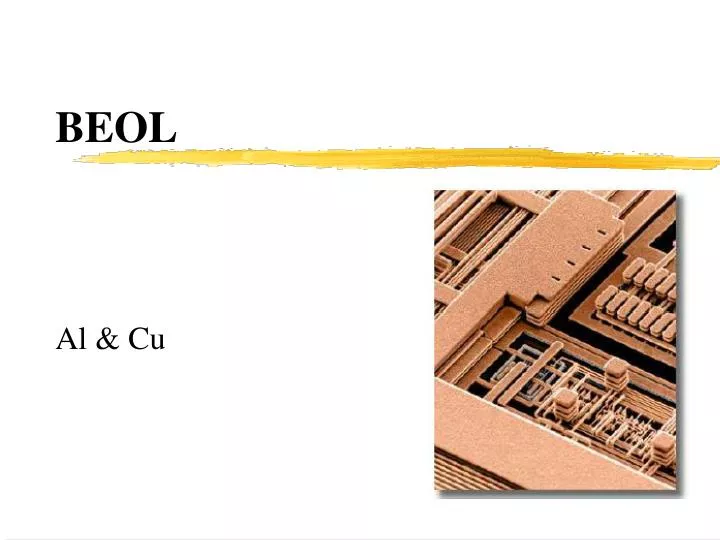
BEOL Al & Cu
Overview • Review • BEOL • Why is it important? • Copper vs Al Technology • Process technology to achieve the final product • Some Integration issues and work-arounds
Electrical Chip Design Physical “Layout” Design R C Testing Creating the chip Chip manufacturing: Snap shot Blue Print- Photo “negative” Review “Print” Quality Control
Metal Contact Device 1 Device 2 Device 3 Device 4 Silicon Wafer Creating the chips Front End of the Line FEOL Back End of the Line BEOL Creating the devices (transistors, capacitors, resistors) Connecting the devices (wiring) Review Packaging
Metal Contact Device 1 Device 2 Device 3 Device 4 Silicon Wafer Chip - Simplified Schematic Review What if you want to connect Device 3 to another device 5 just at the back of Device 3?
Level 2 Level 1 Chip - Simplified Schematic Via Device 1 Device 2 Device 3 Device 4 Silicon Wafer Review Many layers of metal are necessary for current Chips (typically 4 to 5) Up to 8 metal layers are manufacturable in the top class manufacturing units (called fabs)
Intel 7 metal SEM (90 nm node) © Intel
BEOL: Importance Importance has been increasing recently and will continue to do so • For older generation, BEOL was an important factor in the yield of the chip. The speed of the chip was determined by the transistors (FEOL) • What is yield? • More layers than FEOL => more likely to fail. Hence the yield impact For newer generation, BEOL may be important in both yield and speed • Transistors may switch fast, but the signal has to go through wires!
Estimates on delay © www.eedesign.com
BEOL Processes Photo Lithography Deposition (Chemical Vapor Deposition, Physical Vapor deposition, Electrochemical Deposition) Removal (Chemical Mechanical Polishing, Etching) Anneal Review
Overview • Review • BEOL • Why is it important? • Copper vs Al Technology • Aluminum Product : Details • Aluminum/ W Process Flow (partial) • Litho, Dep, Removal • Aluminum process flow (complete) • Cu Process Flow • Process technology to achieve the final product • Some Integration issues and work-arounds
Relevant Conductor Properties • Some of the important & relevant properties • Resistivity (micro ohm-cm) • Litho Process compatibility • eg. Will it react with photo resist? • Melting point • Thermal Expansion coefficient • Diffusivity in silicon di oxide (or any other insulator) • Adhesion to the insulator • Inter-atomic distances (stress) • Process • Crystal orientations, grain sizes • Step coverage
BEOL Materials: Al vs Cu • Conductor: Copper OR Aluminum • Aluminum : Older generation (mostly up to 0.18 um) • Copper: 0.18 um and below • Insulator: • Oxide (silicon-di-oxide) or Low-K materials • What is Low-k? • Low di-electric constant • Why? • Capacitance Metal Metal Via Via Via
Aluminum technology Copper technology Cu Al Cu Cu W W BEOL Materials: Al vs Cu • Low-K: • Being introduced now • Will not be discussed in detail in the class • Few pointers, in the Process Integration chapter • Aluminum and Copper products • Al metal lines are connected by Tungsten Via • Copper lines are connected by copper via
Aluminum technology Al W W Aluminum Process: General • Aluminum Resistivity: 2.6 m ohm-cm • Copper Resistivity: 1.7 m ohm-cm • W Resistivity: 5.7 m ohm-cm • W Via: Why? • Easier to Process • W is higher resistivity, but via is short • ==> Lower impact on the overall resistance
Aluminum technology Al W W Aluminum Process: General • Other relevant information: • Both W and Al need “Liners” • Ti/TiN liners • Diffusion Barriers • Adhesion enhancement • Stress Reduction (==> better reliability)
Aluminum technology Aluminum Process: Detail (a bit) Aluminum technology
Aluminum Process: General Oxide deposition - CVD Shape Definition - Litho Oxide Removal -Dry etch with plasma Ti/TiN Deposition - PVD /CVD W Deposition -CVD W Removal - CMP Ti/TiN Deposition- PVD /CVD Al Deposition PVD Ti/TiN Deposition - PVD/CVD Shape Definition - Litho Ti/TiN/Al Removal - Dry etch with plasma Oxide deposition - CVD
Digression: Intel 7 metal SEM (90 nm node) Pitch = space+width Normally pitch means minimum pitch in a layer Usually M1 pitch is tighter than poly Note M7 is very large (power lines) © Intel
Digression: Metal line widths • M1 is usually very small (eg 200 nm) • M1 pitch is typically tighter than poly pitch M2, M3, etc are slightly larger (eg 250 nm) Last metal (and the last but one) can be very large (eg 400 nm) • Why? • After lot of layers are built, the photo margin tends to be low for small line width/spaces • Last metal tend to carry lot of current and you need the width, to reduce resistance • Fewer wires are needed. Space is available. So why not?
Oxide Deposition Liner Dep (PVD/CVD) Tunsten Dep Tunsten CMP Photo resist coat Litho-Develop Resist Strip Liner Dep Litho-expose Etch CMP Al Dep Aluminum Process: Details (more) Post CMP Clean Densification Other steps: Later on
Copper Process-General • Lower resistivity • Reduced power consumption, reduced heating, longer battery life... • More reliable connection (long term) • Lower processing cost with Dual Damascene • At least, that is the theory! • Faster diffusion • Difficult to etch/ Process not as mature as Al process Damascene Process Single Damascene vs Dual Damascene
Damascene Method Initiated by IBM (practiced in ancient times for pottery designs)
Dep Etch Dep Polish Damascene Method • Example of Single Damascence Process • Single, because one layer is created in one damascene step • Polishing of Copper makes this possible
Etch Dep Etch Polish Damascene Method • Example of Dual Damascence Process • Dual, because two layer are created in one damascene step
CMP Tool: Schematic Controlled Pressure Rotation Rate Controlled slurry flow rate and temp Cu Disk Pad Controlled Rotation Rate Removal is mechanical (abrasive particles) and chemical (dissolution) Inhibitors added for controlled removal
No Removal in this region Removal in these regions CMP removal mechanism Copper Pad ==> non planar surface --> planar surface
CMP: Basics Pressure, Velocity - Removal Rate Chemical Dissolution Controlled Removal ==> Dissolution Inhibitors Smooth Surface ==> Surfactants
BEOL Process-General • Cu or Al process: Liners are present • Cu - Ta/TaN liners • Also has PVD ‘seed’ layer of copper • Al - Ti/TiN liners • Contacts from Transistors to the M1 • Always W • CMP in Cu • newer challenges • Main deposition is Electrochemical • Grain Size (resistivity, electro migration) • void free fill
BEOL Summary • Focus chiefly on conductor (insulator options & processes not discussed in detail) • Al vs Cu processes • Al -etch / Cu Damascene (CMP) • Al -via is W / Cu- via is Cu • Al & Cu: Contact is W • Not all the details of Al vs Cu discussed now • Overall, the processes involved are • Litho, PVD, CVD, Electrochem Dep, Etch, Anneal • Comparison: Production of a chemical: Flow sheet, unit operations