Download

1 / 36
360 likes | 490 Views
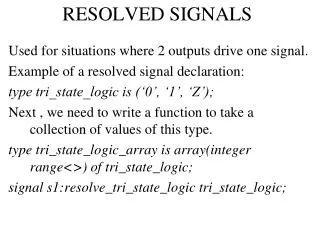
Resolved Signals. Instructors: Fu-Chiung Cheng ( 鄭福炯 ) Associate Professor Computer Science & Engineering Tatung University. Resolved Signals. The final value of a signal driving from two or more different outputs should be resolved based on some analog circuit theory.

E N D
Resolved Signals Instructors: Fu-Chiung Cheng (鄭福炯) Associate Professor Computer Science & Engineering Tatung University
Resolved Signals • The final value of a signal driving from two or more different outputs should be resolved based on some analog circuit theory. • The signal driven to some intermediate state, depending on the drive capabilities of the conflicting drivers • The immediate state may or may not represent a valid logic state • VHDL uses resolution function to calculate the final signal value from the values of all of its sources
Fig 11.1 type tri_state_logic is ('0', '1', 'Z'); type tri_state_logic_array is array (integer range <>) of tri_state_logic; function resolve_tri_state_logic ( values : in tri_state_logic_array ) return tri_state_logic is variable result : tri_state_logic := 'Z'; begin for index in values'range loop if values(index) /= 'Z' then result := values(index); -- may not be correct see Fig 11.2 end if; end loop; return result; end function resolve_tri_state_logic;
Fig 11.2 package MVL4 is type MVL4_ulogic is ('X', '0', '1', 'Z'); -- unresolved logic type type MVL4_ulogic_vector is array (natural range <>) of MVL4_ulogic; function resolve_MVL4 ( contribution : MVL4_ulogic_vector ) return MVL4_ulogic; subtype MVL4_logic is resolve_MVL4 MVL4_ulogic; type MVL4_logic_vector is array (natural range <>) of MVL4_logic; end package MVL4;
Fig 11.2 package body MVL4 is type table is array (MVL4_ulogic, MVL4_ulogic) of MVL4_ulogic; constant resolution_table : table := -- 'X' '0' '1' 'Z‘-- need a resolution table -- ------------------ ( ( 'X', 'X', 'X', 'X' ), -- 'X' ( 'X', '0', 'X', '0' ), -- '0' ( 'X', 'X', '1', '1' ), -- '1' ( 'X', '0', '1', 'Z' ) ); -- 'Z' function resolve_MVL4 ( contribution : MVL4_ulogic_vector ) return MVL4_ulogic is variable result : MVL4_ulogic := 'Z'; begin for index in contribution'range loop result := resolution_table(result, contribution(index)); end loop; return result; end function resolve_MVL4; end package body MVL4;
Fig 11.3 use work.MVL4.all; entity tri_state_buffer is port ( a, enable : in MVL4_ulogic; y : out MVL4_ulogic ); end entity tri_state_buffer; architecture behavioral of tri_state_buffer is begin y <= 'Z' when enable = '0' else a when enable = '1' and (a = '0' or a = '1') else 'X'; end architecture behavioral;
Fig 11.4 use work.MVL4.all; architecture gate_level of misc_logic is signal src1, src1_enable : MVL4_ulogic; signal src2, src2_enable : MVL4_ulogic; signal selected_val : MVL4_logic; -- resolved signal -- . . . begin src1_buffer : entity work.tri_state_buffer(behavioral) port map ( a => src1, enable => src1_enable, y => selected_val ); src2_buffer : entity work.tri_state_buffer(behavioral) port map ( a => src2, enable => src2_enable, y => selected_val ); … end architecture gate_level;
IEEE std_logic_1164 resolved subtypes • See Fig 11.8
Multiple sources for a simple signal • Multiple concurrent assignments cannot be made on a signal– which values?? • This is analogous to driving a circuit node with more than one gate output. • In hardware, this usually results in smoke or an unknown value • In VHDL, it results in an error message • For example Fig 8.22 on page 287
USE WORK.basic_utilities.ALL; -- FROM PACKAGE USE: qit ENTITY y_circuit IS PORT (a, b, c, d : IN qit; z : OUT qit); END y_circuit; -- ARCHITECTURE smoke_generator OF y_circuit IS SIGNAL circuit_node : qit; BEGIN circuit_node <= a; circuit_node <= b; circuit_node <= c; circuit_node <= d; -- four simultaneous driving values z <= circuit_node; END smoke_generator;
Multiple sources for a simple signal • Multiple drivers is possible only if a resolution exists • The anding resolution function ANDs all its drivers • Performs the AND function two operand at a time a b c d anding circuit_node
Anding resolution function -- USE qit, qit_vector, “AND” from basic_utilities FUNCTION anding ( drivers : qit_VECTOR) RETURN qit IS VARIABLE accumulate : qit := '1'; BEGIN FOR i IN drivers'RANGE LOOP accumulate := accumulate AND drivers(i); END LOOP; RETURN accumulate; END anding;
USE WORK.basic_utilities.ALL; -- FROM PACKAGE USE: qit ARCHITECTURE wired_and OF y_circuit IS FUNCTION anding (drivers : qit_vector) RETURN qit IS VARIABLE accumulate : qit := '1'; BEGIN FOR i IN drivers'RANGE LOOP accumulate := accumulate AND drivers(i); END LOOP; RETURN accumulate; END anding; SIGNAL circuit_node : anding qit; BEGIN circuit_node <= a; circuit_node <= b; circuit_node <= c; circuit_node <= d; z <= circuit_node; END wired_and;
ORing resolution function • Figure 8.28 shows an alternative description for the eight-to-one multiplexer • Use ORing resolution function
USE WORK.basic_utilities.ALL; -- FROM PACKAGE USE: qit ARCHITECTURE multiple_assignments OF mux_8_to_1 IS FUNCTION oring ( drivers : qit_vector) RETURN qit IS VARIABLE accumulate : qit := '0'; BEGIN FOR i IN drivers'RANGE LOOP accumulate := accumulate OR drivers(i); END LOOP; RETURN accumulate; END oring; SIGNAL t : oring qit; BEGIN t <= i7 AND s7; t <= i6 AND s6; t <= i5 AND s5; t <= i4 AND s4; t <= i3 AND s3; t <= i2 AND s2; t <= i1 AND s1; t <= i0 AND s0; z <= t; END multiple_assignments;
Package Resolution Functions • The anding and oring resolution functions are useful when an implicit or explicit AND or OR gate exists at a node where several drives meet. • A third function, wiring, is useful for representation of wiring several signals into a common node.
Wire function for modeling wiring two qit type nodes FUNCTION wire (a, b : qit) RETURN qit IS CONSTANT qit_wire_table : qit_2d := ( ('0','X','0','X'), ('X','1','1','X'), ('0','1','Z','X'), ('X','X','X','X')); BEGIN RETURN qit_wire_table (a, b); END wire;
Wire function for modeling wiring qit_vector nodes FUNCTION wiring ( drivers : qit_vector) RETURN qit IS VARIABLE accumulate : qit := 'Z'; BEGIN FOR i IN drivers'RANGE LOOP accumulate := wire (accumulate, drivers(i)); END LOOP; RETURN accumulate; END wiring;
Wire function for modeling wiring qit_vector nodes (declaration) FUNCTION wiring ( drivers : qit_vector) RETURN qit; SUBTYPE wired_qit IS wiring qit; TYPE wired_qit_vector IS ARRAY (NATURAL RANGE <>) OF wired_qit;
Resolution function in basic_utility package FUNCTION oring ( drivers : BIT_VECTOR) RETURN BIT; SUBTYPE ored_bit IS oring BIT; TYPE ored_bit_vector IS ARRAY (NATURAL RANGE <>) OF ored_bit; FUNCTION oring ( drivers : BIT_VECTOR) RETURN BIT IS VARIABLE accumulate : BIT := '0'; BEGIN FOR i IN drivers'RANGE LOOP accumulate := accumulate OR drivers(i); END LOOP; RETURN accumulate; END oring;
MOS Implementation of Multiplexer • NMOS– switch • Also called pass transistor bi: BLOCK ( si = '1' OR si = 'Z') BEGIN t <= GUARDED ii; END BLOCK; ii si t
MOS Implementation of Multiplexer • 8-to-1 NMOS multiplexer • Fig. 8.34 on page 295 • Wired_qi t multiple sources resolution function (wiring) • Bus must be guarded signals
USE WORK.basic_utilities.ALL;-- FROM PACKAGE USE: wired_qit ARCHITECTURE multiple_guarded_assignments OF mux_8_to_1 IS SIGNAL t : wired_qitBUS; BEGIN b7: BLOCK (s7 = '1' OR s7 = 'Z') BEGIN t <= GUARDED i7; END BLOCK; b6: BLOCK (s6 = '1' OR s6 = 'Z') BEGIN t <= GUARDED i6; END BLOCK; b5: BLOCK (s5 = '1' OR s5 = 'Z') BEGIN t <= GUARDED i5; END BLOCK; b4: BLOCK (s4 = '1' OR s4 = 'Z') BEGIN t <= GUARDED i4; END BLOCK; b3: BLOCK (s3 = '1' OR s3 = 'Z') BEGIN t <= GUARDED i3; END BLOCK; b2: BLOCK (s2 = '1' OR s2 = 'Z') BEGIN t <= GUARDED i2; END BLOCK; b1: BLOCK (s1 = '1' OR s1 = 'Z') BEGIN t <= GUARDED i1; END BLOCK; b0: BLOCK (s0 = '1' OR s0 = 'Z') BEGIN t <= GUARDED i0; END BLOCK; z <= t; END multiple_guarded_assignments; • If si = 1 or si=z then t = ii • If non of si is 1 or z then t =‘Z’ (wire function)
NMOS Implementation of Half-Register Multiplexer • Fig 8.37 on page 298 • Modeling this circuit must take inverter input capacitance into account • t holds charge if all are disconnected • Data t can hold several milliseconds • For Sync. Design half-registers are used for data storage in many application (clock refresh rate) • Circuit shows a register effect • Use REGISTER to model retaining of last value indefinitely
USE WORK.basic_utilities.ALL; -- FROM PACKAGE USE: qit, wired_qit ENTITY multiplexed_half_register IS PORT (i7, i6, i5, i4, i3, i2, i1, i0 : IN qit; s7, s6, s5, s4, s3, s2, s1, s0 : IN qit; z : OUT qit ); END multiplexed_half_register; -- ARCHITECTURE guarded_assignments OF multiplexed_half_register IS SIGNAL t : wired_qit REGISTER; BEGIN b7: BLOCK (s7 = '1' OR s7 = 'Z') BEGIN t <= GUARDED i7; END BLOCK; b6: BLOCK (s6 = '1' OR s6 = 'Z') BEGIN t <= GUARDED i6; END BLOCK; b5: BLOCK (s5 = '1' OR s5 = 'Z') BEGIN t <= GUARDED i5; END BLOCK; b4: BLOCK (s4 = '1' OR s4 = 'Z') BEGIN t <= GUARDED i4; END BLOCK; b3: BLOCK (s3 = '1' OR s3 = 'Z') BEGIN t <= GUARDED i3; END BLOCK; b2: BLOCK (s2 = '1' OR s2 = 'Z') BEGIN t <= GUARDED i2; END BLOCK; b1: BLOCK (s1 = '1' OR s1 = 'Z') BEGIN t <= GUARDED i1; END BLOCK; b0: BLOCK (s0 = '1' OR s0 = 'Z') BEGIN t <= GUARDED i0; END BLOCK; z <= NOT t AFTER 8 NS; END guarded_assignments;
Bus, register and not guarded signals • Bus and register are guarded expression BLOCK (guard_expression) BEGIN Guarded_lhs <= GUARDED rls_values; END;
Output is Z calls resolution function with Null Output is saved does not call the resolution function Output is floating does not call the resolution function
A general n-bit multiplexer • Fig 8.41 on page 302 shows an n-bit mux • Fig 8.42 on page 303 show the testbench • Bus can be replaced with register.
USE WORK.basic_utilities.ALL; -- FROM PACKAGE USE: qit, qit_vector, wired_qit ENTITY mux_n_to_1 IS PORT (i, s : IN qit_vector; z : OUT wired_qit BUS); END mux_n_to_1; -- ARCHITECTURE multiple_guarded_assignments OF mux_n_to_1 IS BEGIN bi: FOR j IN i'RANGE GENERATE bj: BLOCK (s(j) = '1' OR s(j) = 'Z') BEGIN z <= GUARDED i(j); END BLOCK; END GENERATE; END multiple_guarded_assignments;
USE WORK.basic_utilities.ALL; ENTITY mux_tester IS END mux_tester; -- ARCHITECTURE input_output OF mux_tester IS COMPONENT mux PORT (i, s : IN qit_vector; z : OUT wired_qit BUS); END COMPONENT; FOR ALL : mux USE ENTITY WORK.mux_n_to_1 (multiple_guarded_assignments); SIGNAL ii, ss : qit_vector (3 DOWNTO 0) := "0000"; SIGNAL zz : qit; BEGIN ii <= "1010" AFTER 10 US, "Z100" AFTER 20 US, "0011" AFTER 30 US; ss <= "0010" AFTER 05 US, "1100" AFTER 15 US, "000Z" AFTER 25 US; mm : mux PORT MAP (ii, ss, zz); END input_output;
TIME(ns) ii(3:0) ss(3:0) zz ======== ====== ====== == 00000 "0000" "0000" '0' +1 d ...... ...... 'Z' 05000 ...... "0010" ... +1d ...... ...... '0' 10000 "1010" ...... ... +1d ...... ...... '1' 15000 ...... "1100" ... +1d ...... ...... 'X' 20000 "Z100" ...... ... +1d ...... ...... '1' 25000 ...... "000Z" ... +1d ...... ...... '0' 30000 "0011" ...... ... +1d ...... ...... '1'
Inout signal • a <= a AND b AFTER delay;
Inout signal ENTITY one (a : IN BIT; x : INOUT BIT) … ENTITY two (b : IN BIT; y : INOUT BIT) … -- ENTITY three IS END three; ARCHITECTURE connecting OF three IS SIGNAL z : oring BIT; . . . BEGIN c1 : ENTITY WORK.one PORT MAP (a, z); c2 : ENTITY WORK.two PORT MAP (b, z); . END connecting;