Download
1 / 7
70 likes | 75 Views
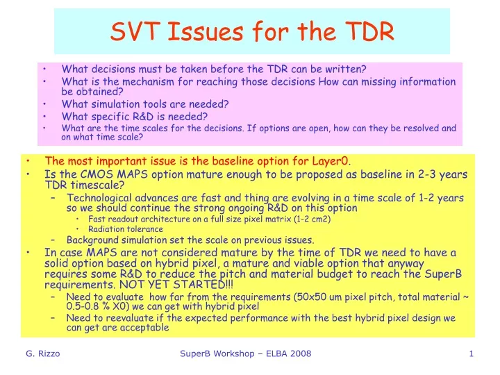
SVT Issues for the TDR. What decisions must be taken before the TDR can be written? What is the mechanism for reaching those decisions How can missing information be obtained? What simulation tools are needed? What specific R&D is needed?

E N D
SVT Issues for the TDR • What decisions must be taken before the TDR can be written? • What is the mechanism for reaching those decisions How can missing information be obtained? • What simulation tools are needed? • What specific R&D is needed? • What are the time scales for the decisions. If options are open, how can they be resolved and on what time scale? • The most important issue is the baseline option for Layer0. • Is the CMOS MAPS option mature enough to be proposed as baseline in 2-3 years TDR timescale? • Technological advances are fast and thing are evolving in a time scale of 1-2 years so we should continue the strong ongoing R&D on this option • Fast readout architecture on a full size pixel matrix (1-2 cm2) • Radiation tolerance • Background simulation set the scale on previous issues. • In case MAPS are not considered mature by the time of TDR we need to have a solid option based on hybrid pixel, a mature and viable option that anyway requires some R&D to reduce the pitch and material budget to reach the SuperB requirements. NOT YET STARTED!!! • Need to evaluate how far from the requirements (50x50 um pixel pitch, total material ~ 0.5-0.8 % X0) we can get with hybrid pixel • Need to reevaluate if the expected performance with the best hybrid pixel design we can get are acceptable SuperB Workshop – ELBA 2008
SVT Design • Design of the SVT support structure and the best way to have the Layer0 easily accessible for replacement. • Important interplay with IR design. • For the external layers the technology is not an issue. • For the TDR need to have a detailed design reoptimizing the geometry for SuperB (several issues raised yesterday no support tube, radial coverage, number of layers) and using the experience of BABAR (arch/wedge detectors in L4-5 were very difficult to be aligned…can we do better?). • Need to evaluate the best front-end chip among the ones “on the market” SuperB Workshop – ELBA 2008
Manpower • How many physicists are involved now? • Some of the physicist from SLIM5 are involved and interest is growing fast… • The group is well motivated but we need more people/groups involved in this R&D hot phase. • How many are needed? When? • First guess: about 6 FTE starting a.s.a.p. • Support for R&D, technical and design personnel? • Very important the support from mechanical and electronic engineer. First guess about 9 FTE needed only ~ 4 FTE involved now. SuperB Workshop – ELBA 2008
backup SuperB Workshop – ELBA 2008
1) Scope of the R&D required (on L0) • Striplets option: mature technology, less robust against background occupancy. • This option become marginal with background rate higher than what stated on CDR ~ 5 MHz/cm2 (Toucheck??) • With present back. estimate moderate R&D needed on module interconnection/mechanics/FE chip (FSSR2) • CMOS MAPS options: new & more challenging technology, more robust against background occupancy. • Extensive R&D needed • Fast readout architecture • Sensor optimization • Radiation hardness • Several mechanical issues: • sensor thinning, module design, power dissipation, light cooling • Hibrid Pixel Option needs to be evaluated more deeply: • An example: Alice hybrid pixel module ~ 1% X0 • Evaluate room for material reduction with the latest technology improvements • Make a fair performance comparison with previous 2 L0 CDR options (in both cases module material ~ 0.5% X0) SuperB Workshop – ELBA 2008
CMOS MAPS R&D goals • TDR time scale: build a prototype multichip MAPS module suitable for application in Layer 0. Demonstrate the ability to build a working detector with this technology. • Present R&D on DNW MAPS very encouraging • Need to demonstrate fast readout architecture implementation is possible with this technology (R=5MHz/cm2, continous beam structure) • Crosstalk due to digital line crossing the pixel seems cured but still some effects are present (power distribution? ) • Scalability of the readout architecture to large matrix (Area ~1 cm2) • 256 pixel matrix produced: test started. - 4k pixel matrix in production Nov. ’07 • Issues for larger matrix: power distribution, output rate. efficiency of the readout • Explore alternative architecture: data driven vs triggered architecture. • Pixel cell optimization to improve S/N, charge collection efficiency, power dissipation. • S/N = 1524, Power=30 mW/ch in chips just received • Evaluate different technology (IBM 130 nm triple well) • Radiation tolerance: tests performed on CMOS MAPS from other groups indicate adequate rad. hardness for SuperB. Some effects are design/process dependent needs to be investigated on our DNW MAPS. • Irradiation program just started • Optimize pixel cell for radiation hardness SuperB Workshop – ELBA 2008
MAPS module proposed (AlN support + minichannel with cold liquid) • Two MAPS layers (up/down) placed on the mechanical support forming a ladder. • Each chip: 12.8mm x 12.8mm. • Total Layer0 thickness: 0.5 % X0 • 0.1 % (Si) + 0.3 % (Supp+Cooling) + 0.1 % (bus/Cu) Mechanics & Module design R&D • MAPS power dissipation is large (in the active area!) • Power = 50 μW/cell = 2 W/cm2 • Power dissipation drives the mechanical problem • FEA for MAPS module proposed indicates power evacuation possible with a support/cooling thickness ~ 0.3% X0: • Extensive R&D activity on microcooling • See F. Bosi’s talk at the SVT parallel session. • Need to demonstrate feasibilty with meas. on mechanical prototype • Thermoidraulic Testbench in prep. for accurate thermic measurements • Mechanincal activity also to optimize the design of the striplets option. SuperB Workshop – ELBA 2008