Download
1 / 19
210 likes | 562 Views
Design and Scaling of SiGe BiCMOS VCOs Above 100GHz. S. T. Nicolson 1 , K.H.K Yau 1 , K.A. Tang 1 , P. Chevalier 2 , A. Chantre 2 B. Sautreuil 2 , and S. P. Voinigescu 1 1) Edward S. Rogers Sr. Dept. of Elec. & Comp. Eng., Univ. of Toronto 2) STMicroelectronics. Outline.

E N D
Design and Scaling of SiGe BiCMOS VCOs Above 100GHz S. T. Nicolson1, K.H.K Yau1, K.A. Tang1, P. Chevalier2, A. Chantre2B. Sautreuil2, and S. P. Voinigescu1 1) Edward S. Rogers Sr. Dept. of Elec. & Comp. Eng., Univ. of Toronto 2) STMicroelectronics
Outline • Motivation for W-band SiGe integrated circuits • VCO design methodology for low phase noise in W-band • Layout considerations • Measurement results • Conclusions and future work
Motivation for W-band SiGe ICs • Typical applications: 77GHz auto radar, 94GHz weather radar, imaging • Central to these applications is the low phase noise VCO • Process development: NFmin, Rn & Ysopt difficult to measure in W-band • Use VCO as a process monitor for the noise performance of SiGe technologies • Explore VCO scaling/yield in SiGe
2.5 V VCC LC CM LB Q1 VBB Cext VTUNE+ Cvar LEE VTUNE- REE CEE RB B C cp rp bib Cext VTUNE E VCO Topology • No cascode • lower phase noise, lower supply voltage • Colpitts topology • maximize fosc relative to other topologies • Augment Cbe with Cext • Reduces phase noise • Add negative Miller capacitors • Increases fosc by cancelling Cm • Differential tuning • reduces supply induced noise 24mA
W-Band VCO Design Methodology • Use smallest realizable LB with adequate Q • Given fosc, maximize tuning range using large Cext • Negative resistance • Phase noise formula • Phase noise trade-off when HBT pushed to limit • Minimize HBT noise bias at NFmin current density • Maximize Vtankand Cext bias at peak fT current density Max. Rneg occurs atpeak fT/fMAX bias
VCO Fabrication BipX1fT = 270GHzfMAX = 260GHz emitter4×5mm×0.13mm • Fabricated in three technology splits: • All VCO layouts and bias currents are identical – no redesign • Directly compare VCOs fabricated in different processes • Use the VCO to optimize HBT profile • Noise parameters from phase noise • fMAX from VCO output power BipXfT = 230GHzfMAX = 300GHz emitter4×5mm×0.13mm BiC9fT = 150GHzfMAX = 160GHz emitter4×5mm×0.17mm
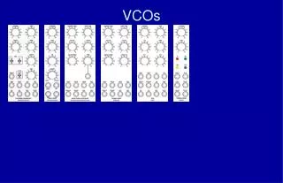
70mm 100mm VCO Layout • VCO core area: 100mm × 100mm • Spiral inductors where necessary to reduce area • Plenty of supply decoupling (MiM and metal-metal)
Technology Overview – fT/fMAX Scaling • Peak fT/fMAX current density increases at each technology node • 0.17mm SiGe JpeakfT = 7mA/mm2 where fT = 150GHz • 0.13mm SiGe JpeakfT = 14mA/mm2 where fT = 230GHz (or 250GHz) • Contrast with CMOS… • JpfT = 0.3mA/mm, JpfMAX = 0.2mA/mm, JNFmin = 0.15mA/mm for 180-65nm nodes
Measurement Results • VCO performance comparison in 3 SiGe technologies • Phase noise performance • Temperature testing • Wafer mapping
Performance Comparison Across Technology • LC-oscillator frequency insensitive to technology fT/fMAX • MOS varactors give less phase noise than HBT (CBC) varactors • Higher fMAX more output power, higher frequency • BipX1 results in lowest phase noise
Phase Noise Performance • Oscillation frequency of 104GHz • Phase noise of 101.3dBc/Hz @ 1MHz offset Phase Noise in W-Band SiGe VCOs FMCW modulation Averaged Spectral Plot **References provided in abstract**
RB C B bib cp <inB> <inC> E Biasing W-Band VCOs for Low Noise • NFmin current density scales with technology and fosc • Emitter width JNFmin (scales with JpeakfT) • Frequency JNFmin (gets closer to JpeakfT) • Noise correlation further increases JNFmin [K. Yau, SiRF, 2006] The B and C shot noise currents are correlated
output power 2.5 V VCC LC CM phase noise LB Q1 VBB Cext JNFMIN increases with frequency VTUNE+ Cvar LEE VTUNE- REE CEE Phase Noise Performance Across Bias • What is the minimum phase noise current density in W-band VCOs? • Measure output power and phase noise w.r.t current density (vary VBB) • Looks like phase noise is minimum at peak fT current density
25ºC 25ºC 25ºC 70ºC 70ºC 125ºC BiC9 MOS var. 50ºC BiC9 HBT var. BipX W-Band Manufacturability Challenges • Manufacturability specifications for automotive radar are stringent • Outdoors wide temperature variations • Must last for car’s lifetime • Low cost per part requires high yield • Is SiGe on the way to meeting such challenges?
Wafer Mapping – BiCMOS9 • Tested 120 VCOs on 4 wafers • Summary of BiC9 VCOs with MOS varactors (60 dice averaged) • Summary of BiC9 VCOs with HBT varactors (60 dice averaged) • 4 VCOs had significantly below average performance (outliers) • 2 of the 4 outlier VCOs failed to oscillate entirely
Oscillation Frequency Phase Noise at 1MHz offset Wafer flat Location of VCO in reticule VCO not present VCO not present Die not tested Die not tested 104.5-105.0 GHz < -98 dBc/Hz 104.0-104.5 GHz -95 – -98 dBc/Hz 103.5-104.0 GHz -92 – -95 dBc/Hz 103.0-103.5 GHz > -92 dBc/Hz Wafer Mapping – BipX
Figures of Merit • Comparison of our work to other state of the art W-Band VCOs References [1] Huang P. et al, ISSCC 2006 [2] Kobayashi K. W. et al, JSSC 1999 [3] Tang K. W. et al. CSICS 2006 [4] Huang P. et al, ISSCC 2006
Conclusions • Demonstrated a design methodology for low phase noise in W-Band VCOs • Biasing at JpeakfT minimizes phase noise in W-band VCOs • Performed a direct comparison of identical VCOs fabricated in different technologies • LC-oscillator frequency is insensitive to technology scaling • Higher fT technology yielded VCO with lower phase noise • Higher fMAX technology yielded VCO with improved output power • Future work is required to fully support these conclusions • Noise figure measurements in the W-Band (correlate to Y-parameter method) • Verify JNFmin in the W-Band and support biasing near JpeakfT for min. phase noise
Technology Overview – fT/fMAX Scaling • Improvement in peak fT/fMAX has two contributions • Layout stripe contact, decreased emitter width 0.17mm to 0.13m • Vertical profile and processing doping, materials, epitaxy, etc. • How much of the speed improvement is due to each contribution? • Measure the 0.13mm HBT layouts fabricated in the 0.17mm process