Download
1 / 12
120 likes | 212 Views
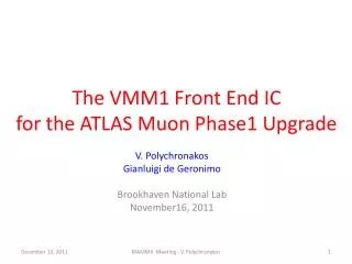
VMM Update Front End ASIC for the ATLAS Muon Upgrade. V. Polychronakos BNL. Design Parameters/Features. Dual Polarity Adjustable Gain (0.5 – 9.0 mV/ fC ) Adjustable peaking Time (25-200 ns) Address in Real Time (Fast OR in effect - Mmegas Trigger)

E N D
VMM UpdateFront End ASIC for the ATLAS Muon Upgrade V. Polychronakos BNL RD51 - V. Polychronakos, BNL
Design Parameters/Features • Dual Polarity • Adjustable Gain (0.5 – 9.0 mV/fC) • Adjustable peaking Time (25-200 ns) • Address in Real Time (Fast OR in effect - Mmegas Trigger) • Prompt digitized (6-bit) Amplitude, Time-over-threshold, time-to--peak (TGC Trigger) • Peak Detector, Time Detector (<1 ns) • Discriminators with sub-hysteresis • Neighbor enable logic (channel to channel and across Ics) • Sparse readout w/smart token passing, • Threshold trim, built-in calibration, channel mask, analog monitor, temp. sensor, 600 BGR, 600 mV LVDS RD51 - V. Polychronakos, BNL
VMM1, First Version, 64 channels, fully functional analog front end, Amp, Timing analog multiplexer outputs RD51 - V. Polychronakos, BNL
Signal Processing Concept • Discriminators Data driven front end • Zero suppression • Neighbor Logic (channel to channel and across chips) allows processing below threshold signals • Peak Detector provides signal amplitude • Peak timing with negligible time walk and excellent resolution • Discriminators with sub-hysteresis feature allow trigger at a few mV above baseline RD51 - V. Polychronakos, BNL
Timing +1 BCID Start of live spill triggers 40 MHz clock Time to Analog converter starts at “peak found”, marks the hit time wrt leading edge of BCID TAC stops at rising edge of BCID+2 (125 ns ramp) TAC amplitude digitized by 8-bit ADC HIT time = BCIDx25 + ADC*125/256 [nsec] BCID and ADC are stored in buffer Process repeated for subsequent hits Could do away with ramp, have, e.g., 200 MHz clock and just record BCID count (5 ns resolution) RD51 - V. Polychronakos, BNL
Examples of VMM1 performance ENC as a function of input capacitance <1fC even with fast shaping (25 ns) and large input capacitance (200 pF) Time resolution as a function of amplitude ~ ns resolution and timewalk RD51 - V. Polychronakos, BNL
Sub-hysteresis allows trigger at very low Amplitudes Allows setting trigger threshold at 1 or 2 primary electrons RD51 - V. Polychronakos, BNL
The Second version of the ASIC (VMM2) • Fixes issues (mostly minor) of the first version • Includes 10-bit digitizers for amplitude and timing (200 ns) • Includes a 6-bit Amplitude digitizer at ~40 ns conversion time • Includes 4 word buffer, simultaneous read/write, can continuously be read out at both phases of 200 MHz clock in DDR mode 800 Mbps G. De Geronimo, BNL Instr. Div. IBM 8RF 130 nm CMOS process, 1.2 V 9.1 x 9.1 mm2, ~6.5 mW/channel RD51 - V. Polychronakos, BNL
VMM2 Readout (May be modified in final version) 4-deep buffer 200 MHz Clock Uses both phases Effectively 800 Mbps RD51 - V. Polychronakos, BNL
Trigger Feature 1- Address in Real Time (ART) At every bunch crossing ART provides the 6-bit address of the channel with the earliest signal above threshold Can be used as a fast OR RD51 - V. Polychronakos, BNL
Trigger Feature 2- Prompt 6-bit amplitude per Channel RD51 - V. Polychronakos, BNL
Summary, Schedule - Availability • VMM2 design completed about a month ago • Layout, simulations in progress, expect to be completed end of November (next MOSIS MPW run) • VMM is a very large chip (~ 100 sq.mm), cost 230 k$US/40 samples! • Decided to go for a dedicated run (450 k$US) sharing the wafer with a smaller BNL ASIC which will reduce the cost by ~ 100 k • The cost above includes processing of 6 wafers, ~800-1000 chips • Chips available ~May 2014 if submitted in early December • Package in BGA 350 pins (21x21 mm2) • In the process of applying for Commerce Department export license • What remains for the final version is SEU mitigation logic and final decision on digital buffer size and management • Several Readout boards for ATLAS under development, SRS compatible hybrid under discussion RD51 - V. Polychronakos, BNL