Download
1 / 29
370 likes | 860 Views
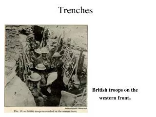
Trenches…. Chris Seymore. Questions…. What are the two difficulties associated with Etching Trenches? How does doping occur in trenches where the trench width is smaller than the thickness of the plasma sheath?. Overview. Etching a trench

E N D
Trenches… Chris Seymore
Questions… • What are the two difficulties associated with Etching Trenches? • How does doping occur in trenches where the trench width is smaller than the thickness of the plasma sheath?
Overview • Etching a trench • Quick Review of Ion Beam Implantation and Plasma Immersion Ion Implantation • Doping a trench • Filling a trench • Conclusion
Etching a Trench • Mask off areas on the surface • Done with liquid chemicals in the past • “Directionally Blind” • Modern Transistors led to need for trenches with vertical walls • Plasma Etching-very directional • Great for getting the clean sides and bottoms which work best for transistor junctions http://www.nas.nasa.gov/Main/Features/2000/Fall/plasma.html
Cutting the Trench (cont) • Use chemical (Cl containing gas) • Reactive radicals chemically react with Si creating volatile products to be pumped away • Mechanical (Ion bombardment) • Sputter material away • Hybrid (Reactive Ion Etcher) • Passivation- molecular Cl reacts with Si • Ion Bombardment knocks away the resulting Silicon Chlorides • Good for low aspect ratio (<3) http://www.nas.nasa.gov/Main/Features/2000/Fall/plasma.html http://www.soiplus.com/technical_articles/125285225TrenchTechnology.pdf
Deep Reactive Ion Etch (DRIE) -High Density Inductively Coupled Plasma -Aspect Ratio up to 30:1 -Sidewall Angles 90 +/- 2 -Etch Rate up to 10 micro meter/ min -SF6 and C4F8 gases used http://www.inex.org.uk/page.asp?pageid=77 http://www.protron-mikrotechnik.de/technology/technology_ase_e_2.htm
Tools to help with Etching • Obtaining ideal trench w/ fast etch rate difficult • Right number of neutral and energetic ions • Size of the trench opening • Controlling the direction, speed and angle of the ions • Current (2000) gen transistors measure .18 microns • NASA are developing a simulation tool to model trench etching • Goal to determine optimal conditions (ie Operating Power, Pressure, material properties) for creating ideal trenches • Simulation of Profile Evolution using Level Sets (SPELS) • New discovery…Hydrogen Bromide produces better trenches than those made with Chlorine http://www.nas.nasa.gov/Main/Features/2000/Fall/plasma.html
Difficulties of Trench Cutting… • Microtrenching Bowing http://www.nnf.cornell.edu/2000REU/pdf/Mordovanaki.pdf
Microtrenching Dependence on Aspect Ratio • Setup: • ICP High Density Plasma Etcher (Lam 9600) Using HBr at 250W • ICP good for independent control of plasma density and bias voltage • Bias Power at 60W • Bias Voltage 104V • Etch Time 540s • Low Pressure (10mT) • Lower the Aspect Ratio, lower the Microtrenching http://www.nnf.cornell.edu/2000REU/pdf/Mordovanaki.pdf
Effect of increased energy… • Setup: • ICP High Density Plasma Etcher (Lam 9600) Using HBr at 250 and 500W • Bias Power 60 and 150W • Bias Voltage at 104 and 93V • Etch Time 540s • Low Pressure (10mT) • Higher Energy cleaned up the microtrenching, but increased the bowing. Low Energy High Energy http://www.nnf.cornell.edu/2000REU/pdf/Mordovanaki.pdf
Conclusions of the Experiments • They believe that the original microtrenching was caused by reflections of the ions off the side walls • They did state that they ran short in their experiment time and weren’t fully able to characterize the results they saw • Doesn’t make sense to me because…when they saw micro trenching, they had no bowing • Why when the bias power was increased…they saw more bowing?
Ion Beam vs Immersion http://silver.neep.wisc.edu/psii/
Trench Doping • Experiment in 1990 showed it impossible to dope trenches w/ Ion Beam Implantation • In 1994 another group tried with Plasma Immersion Ion Implantation • Use RF Plasma of dopant gas • Add bias to the substrate • One problem…trench widths smaller than Ion sheath Handbook of Plasma Immersion Ion Implantation and Deposition, Andre Anders ed. Published by Wiley-IntersciencePage,2000, pg 667-669 http://ieeexplore.ieee.org/iel1/55/7136/00286690.pdf?isNumber=7136&arnumber=286690&prod=JNL&arSt=196&ared=198&arAuthor=Crid+Yu%3B+Chenng%2C+N.W.
Trench Doping (cont) • Experiment Setup • BF3 Plasma • Trench Widths of 1,2, and 5 micrometer • Trench Depths of 5 and 10 micrometer • Bias Voltages from 2-10kV • Pressure 5mT • Bias pulse 1micro s duration at rate from 200-1000Hz • 1000 C for 60 minutes • Compared the Sidewall Dose with the Surface Dose • Results • Can dope trenches with this process with AR up to 15 • Better at lower bias voltage for conformal coverage • Dependant on angular distribution of ions Handbook of Plasma Immersion Ion Implantation and Deposition, Andre Anders ed. Published by Wiley-IntersciencePage,2000, pg 667-669 http://ieeexplore.ieee.org/iel1/55/7136/00286690.pdf?isNumber=7136&arnumber=286690&prod=JNL&arSt=196&ared=198&arAuthor=Crid+Yu%3B+Chenng%2C+N.W.
Trench Filling Pictures 5kV Bias Voltage 10kV Bias Voltage
Trench Filling • Metallic Filling (wires and vias) • Oxide Filling (DRAM Gap Fill)
Oxide Trench Filling • Needed to fill Doped Trenches • HDP-CVD is the major technique for deposing oxide dielectric films • As ICs shrink in size, gap fill requirements become more aggressive due to higher aspect ratio of the features • HDP-CVD-sputtering and deposition take place simultaneously • Redeposition on sidewall closes off trench…gaps A Novel NF3-HDP_CVD Process for STI-Flilling in Sub-90nm DRAM and Beyond, Yon-Won Cha, Sang-Ho Rha, Won-Jin Kim, Kyu-Tae Na, U-In Chung, Joo-Tae Moon
Oxide Trench Filling (cont) • In order to remove the re-deposited film, an investigation was done by adding NF3 to the SiH4 and O2 • New process called NF3 –HDP-CVD A Novel NF3-HDP_CVD Process for STI-Flilling in Sub-90nm DRAM and Beyond, Yon-Won Cha, Sang-Ho Rha, Won-Jin Kim, Kyu-Tae Na, U-In Chung, Joo-Tae Moon
NF3 –HDP-CVD Experiment • Setup • 200mm Ultima-X HDP-CVD Centura System • 1st with SiH4 and O2 only • 2nd with NF3 , SiH4 and O2 • Pressure 3-5 mT • Oxide Deposition Rate of 400-700 nm/min • Trench 70nm opening/350 nm depth • One concern…When adding the NF3 could damage the Nitride layer of the STI A Novel NF3-HDP_CVD Process for STI-Flilling in Sub-90nm DRAM and Beyond, Yon-Won Cha, Sang-Ho Rha, Won-Jin Kim, Kyu-Tae Na, U-In Chung, Joo-Tae Moon
NF3 –HDP-CVD Experiment (cont) • Results • The addition of the NF3 showed better oxidation fill and less gaps • Nitride layer wasn’t damaged because the deposition rate was higher than the etch rate • One problem…Abnormal Layer at Trench Sidewall (ALTS) • Think it is caused by re-deposition and fluorine impurities • Cleared up with High Temperatures because they allowed the F to diffuse to the other regions • Temperature is related to Bias Voltage…simple enough, just increase the bias voltage to clear up the ALTS…not so fast • Higher Bias Voltage also damages the pattern due to high sputtering rates (ie clipping) A Novel NF3-HDP_CVD Process for STI-Flilling in Sub-90nm DRAM and Beyond, Yon-Won Cha, Sang-Ho Rha, Won-Jin Kim, Kyu-Tae Na, U-In Chung, Joo-Tae Moon
Pictures of the Results SiH4 and O2 only Voids present NF3, SiH4 and O2 No Voids Present, But ALTS are present NF3, SiH4 and O2 at higher OSR; No Voids or ALTS present A Novel NF3-HDP_CVD Process for STI-Flilling in Sub-90nm DRAM and Beyond, Yon-Won Cha, Sang-Ho Rha, Won-Jin Kim, Kyu-Tae Na, U-In Chung, Joo-Tae Moon
More Results • Sputtering Rate… • Direct relationship to the Bias Voltage • Previously, it had been well accepted that an increase in Oxygen result in higher sputtering rate • Found that there is a point where the sputtering decreases because the mean free path of the sputtering ions becomes shorter • Found that a Bias of around 2660 W and an Oxygen to Silicon Ratio of 1.8 produced best performance A Novel NF3-HDP_CVD Process for STI-Flilling in Sub-90nm DRAM and Beyond, Yon-Won Cha, Sang-Ho Rha, Won-Jin Kim, Kyu-Tae Na, U-In Chung, Joo-Tae Moon
Metallic Trench Filling • The need to “wire” the internal elements of the new minituraized ICs presents the need to develop a method of Trench Filling • Originally Aluminum and Tungsten • Now Copper preferred • Low Resistivity allows for finer wires • High melting point makes it less susceptible to electromigration Handbook of Plasma Immersion Ion Implantation and Deposition, Andre Anders ed. Published by Wiley-IntersciencePage,2000, pg 669-673
Trench Filling (cont) • Conventional Physical Vapor Deposition (ie sputter deposition and evaporation) failed to fill trenches with high AR • Better filling techniques include Collimated Sputtering, Self-Sputtering, ECR or Vacuum Arc Plasma • Still unable to fill trenches with AR >4:1 (<180nm wide) • Inadequate control over particle velocity distribution and Ion energy Handbook of Plasma Immersion Ion Implantation and Deposition, Andre Anders ed. Published by Wiley-IntersciencePage,2000, pg 669-673
Combined Filtered Cathodic Arc and PIII • Also known as MePIIID • Growth rate is dependent on deposition versus sputtering • Why is this so good? • High directionality of Ion Flux • Tight control of Energy of Depositing Ions Handbook of Plasma Immersion Ion Implantation and Deposition, Andre Anders ed. Published by Wiley-IntersciencePage,2000, pg 669-673
Ion Deposition • Conventional-Growth rate is dependent on ratio of Ions to neutral particles • The Ion Energy is the sum of the streaming energy and the energy added by the applied bias voltage. E=E0+ZeVbias • E0 is the streaming energy (approx 90eV for Cu) • Z is the mean ion charge (2 for Cu) • e is the electron charge (1.60 X10⁻¹⁹) Handbook of Plasma Immersion Ion Implantation and Deposition, Andre Anders ed. Published by Wiley-IntersciencePage,2000, pg 669-673
Combined Filtered Cathodic Arc and PIII (cont) • Filled trenches with widths as small as 100nm with AR up to 9:1 Bad Trench Fill Good Trench Fill Handbook of Plasma Immersion Ion Implantation and Deposition, Andre Anders ed. Published by Wiley-IntersciencePage,2000, pg 669-673
Conclusion • Trench Etching • Trench Doping • Trench Filling
Answers • What are the two difficulties associated with Trench Etching? • Micro-trenching • Bowing • How does doping occur in trenches where the width is smaller than the plasma sheath? • The Bias voltage must be low enough so that ions get more angular acceleration due to collisions with neutral particles