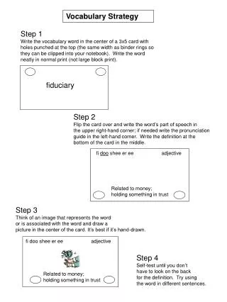
Download
1 / 13
140 likes | 293 Views
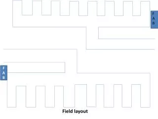
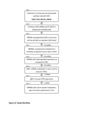
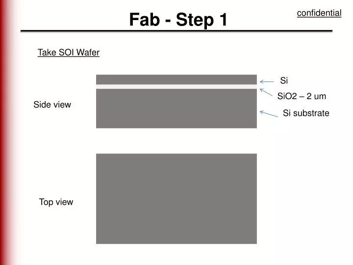
confidential. Fab - Step 1. Take SOI Wafer. Si. SiO2 – 2 um. Side view. Si substrate. Top view. confidential. Fab – Step 2. Grow thermal oxide. Si. SiO2 – 2 um. Side view. Si substrate. Top view. confidential. Fab – Step 3. Dry etch thermal oxide from the front of the wafer.

E N D
confidential Fab - Step 1 Take SOI Wafer Si SiO2 – 2 um Side view Si substrate Top view
confidential Fab – Step 2 Grow thermal oxide Si SiO2 – 2 um Side view Si substrate Top view
confidential Fab – Step 3 Dry etch thermal oxide from the front of the wafer Si SiO2 – 2 um Side view Si substrate Top view
confidential Fab – Step 4 Deposit AlN AlN Si SiO2 – 2 um Side view Si substrate Top view
confidential Fab – Step 5 Etch AlN to define the structure – Mask 1 AlN Si SiO2 – 2 um Side view Si substrate Top view
confidential Fab – Step 6 Deposit Pt Pt Si SiO2 – 2 um Side view Si substrate Top view
confidential Fab – Step 7 Etch Pt – Mask 2 Si SiO2 – 2 um Side view Si substrate + Q +/- Q Top view - Q
confidential Fab – Step 8 Etch Si to define the structure – Mask 3 Si SiO2 – 2 um Side view Si substrate + Q +/- Q Top view - Q
confidential Fab – Step 9 Etch buried oxide to define the structure – Mask 3 Si SiO2 – 2 um Side view Si substrate + Q +/- Q Top view - Q
confidential Fab – Step 10 Spin coat protective photoresist and bake it Photoresist Si SiO2 – 2 um Side view Si substrate + Q +/- Q Top view - Q
confidential Fab – Step 11 Pattern back oxide to be used as hard mask for back side etch – Mask 4 Photoresist Si SiO2 – 2 um Side view Si substrate + Q +/- Q Top view - Q
confidential Fab – Step 12 Back side etch of Si – Mask 4 Photoresist Si SiO2 – 2 um Side view Si substrate + Q +/- Q Top view - Q
confidential Fab – Step 13 Strip photoresist Si SiO2 – 2 um Side view Anchor Si substrate + Q +/- Q Top view - Q