Download
1 / 22
220 likes | 228 Views
3D STEM Imaging. EM Technologies and prospective issues in 3D STEM imaging. Research Presentation, The University of Tennessee, Knoxville. by Muharrem Mercimek 7 Feb. 2007. About this Presentation. Need for nano-imaging Atomic material cauterization benefits. SEM, TEM, and STEM

E N D
3D STEM Imaging EM Technologies and prospective issues in 3D STEM imaging Research Presentation, The University of Tennessee, Knoxville. by Muharrem Mercimek 7 Feb. 2007
About this Presentation • Need for nano-imaging • Atomic material cauterization benefits. • SEM, TEM, and STEM • Experimental Issues • Limitations, factors affect the results • Common STEM signals • HAADF, ADF, BF images, • EDX, EEL spectrums • 3D Nano-Imaging • Confocal Imaging, • Depth Sectioning, • Some solutions to the Problem • ORNL team’s achievements • Prospective researches
Need for nano-imaging • Images and quantitative data at the level sub-Ångstroms are invaluable; for structure determination, mass mapping of the bimolecular structures. • The possibility of identifying, localizing single atoms represents the ultimate advance for understanding the atomic origins of materials’ properties. • Revealing atomic arrangements are indispensable for 1-first principles calculations, 2-chemical reactivity measurements, 3-electrical properties, 4-point defects, 5-optical properties
SEM, TEM, and STEM • Conventional light microscopes use a series of glass lenses to bend light waves and create a magnified image. • The electron microscopes EM creates the magnified images by using electrons instead of light waves. • Scanning Electron Microscope SEM • scans the electron beam across the sample • no lenses below the sample • detection of reflected electrons. • SEM images are the easiest of these three to interpret. • Transmission electron microscope TEM • passes a beam of electrons through the sample, • has image forming lenses which create a direct image of a viewing screen, • detection of transmitted electrons • the image of the sample is recorded at once
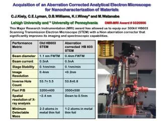
SEM, TEM, and STEM • A scanning transmission electron microscope STEM • is a type of TEM, detection of transmitted electrons, • the electrons pass through the specimen, • as in SEM, the electron optics focus the beam to obtain an electron probe is scanned over the sample • The essential difference between the optics of a STEM and a TEM • In TEM a large area of the sample is illuminated and the significant magnification is performed by the lens system after the specimen, allowing the whole image to be recorded at once. • In STEM, the focusing is done before the electrons reach the specimen to form a very tiny probe which is scanned over the sample. • TEM: JEOL JSM-3100F Point resolution 1.7 Angstrom • SEM: JEOL 7700F Point resolution 6.0 Angstrom • STEM: VG HB603U with Nion Aberration Corrector Point resolution 0.6 Angstrom
SEM, TEM, and STEM TEM http://nobelprize.org/educational_games/physics/microscopes/tem
SEM, TEM, and STEM SEM http://acept.la.asu.edu/PiN/rdg/elmicr/elmicr.shtml
SEM, TEM, and STEM STEM http://vpd.ms.northwestern.edu/teaching/teaching466.htm
Experimental Issues in EM • Scan time cannot be made arbitrarily long, because of the variations which occur in lens currents and accelerating voltages. • When high accelerating voltage is used image sharpness and the resolution will be better. • The smaller the probe current the sharper the image, but the surface smoothness is lost. • The smaller the electron probe diameter on the specimen the higher the magnification and the resolution. • If the depth of the sample increases, the electron probe gets wider and resolution decreases. • The biological samples should be dried and covered with a very thin metal layer, such as gold layer.
Common STEM signals • HAADF-High angle annular dark field images • ADF- Annular dark field images • BF-Bright Field Images. • Secondary Electrons • Backscattered Electrons • Energy-dispersive X-ray (EDX) spectrum • Electron energy loss spectrum Scattered and unscattered electrons HAADF:(Θ > 3°), BF: ADF (Θ = 0.5°-3°) Dark Field and Bright Field STEM Images
STEM EDX Specimen ADF EELS Common STEM signals • HAADF can also be referred as Z-contrast mode. • Atomic resolution Z-contrast image is a convenient and intuitive method for revealing atomic arrangements. • EELS requires specimens to be less than 20-30 nm. • ADF is an imaging mode where metal particles are bright. • BF is an imaging mode where the fringes can be seen when substrate flakes are in focus. • For Z-contrast mode Brightness is proportional to square of atomic number →Z2. • 0.74130Å bond distance of H-H, Z=1, • 1.20741 Å bond distance of O-O, Z=8. • 2.35200 Å bond distance of Si-Si, Z=14 • 5.30900 Å bond distance of Cs-Cs, Z=55
3D Nano-Imaging • (3D Tomography in STEM) • The STEM’s Z-contrast mode images gives an incoherent image of the sample making it possible to optically section through a sample in a way similar to confocal optical microscopy. • However in STEM there is no pin-hole conjugate to the focal point of the lens. • Problems: • Focal depth generally is the bottleneck of the 3D resolution • Depth sensitivity is about electron probe BUT estimations about depth sensitivity is not directly related to focal depth and vertical resolution. • Propagation of the beam through the sample results in a simple broadening of the probe. Optical sectioning of a sphere by confocal planes 1 Rejection of light not incident from the focal plane 2 1- http://www.loci.wisc.edu/optical/sectioning.html 2-http://www.physics.emory.edu/~weeks/lab/papers/ebbe05.pdf
3D Nano-Imaging • Optical sectioning • if thick slices are examined, structures in the interior of the specimen are usually obscured by interference from structures at either side of the plane of focus. • Several stacks of images can be automatically acquired by translating the microscope and by exploiting the focus drive. • This is an iterative computational technique in which a stack of focal sections is recorded and the contribution of out-of-focus signal to a given section from structures in other sections is computed and subtracted from that section.
Some solutions to the Problem • 130 micrographs with 1024 x 1024 or 2048 x 2048 pixels were acquired automatically over a tilt-range of ±75° using the Saxton scheme. The magnification typically corresponds to a pixel size of 0.25 – 1 nm at the specimen level resulting in a total field of view of about 0.3 – 2 μm. • Inspect3D or IMOD were used to align the tilt-series by cross-correlation followed by marker tracking to refine the relative image shifts, magnification, and tilt-axis orientation. [Christian Kübel, Jennifer Kübel, Stephan Kujawa, Jian-Shing Luo, Hui-Min Lo, Jeremy D. Russell, “Application of Electron Tomography for Semiconductor Device Analysis”,AIP Conference Proceedings 817, page 223-228, American Institute of Physics, Melville, New York, 2006.] • Modifying the standard 2D incoherent-imaging convolution formalism used to described Z-contrast STEM to accommodate 3D imaging. Channeling of the probe plays an important role in 3D imaging. The transmission function is a collection of Dirac functions at the atom positions ri, weighted by the atomic number of each atom Zi; and the image is a 3D convolution of these two • P(r): the incident probe intensity. This results in a 3D image I(r), which is measured one 2D plane at a time by changing the objective lens defocus f. [Paul M. Voyles, “Imaging Single Atoms with Z-Contrast Scanning Transmission Electron Microscopy in Two and Three Dimensions”, Chemistry and Materials Science Issue Volume 155, Numbers 1-2, September, 2006]
Some solutions to the Problem • 3D data collection using STEM from various directions. • Topographic reconstruction model is used. • Surface shape is obtained using corresponding surface points between stereo images. • A closed curve is extracted from several 2D images. In 3D space the curve is swept along the direction of projection. • Cylindrical specimens were prepared. • [M. Koguchi, H. Kakibayashi, R. Tsuneta, M. Yamaoka, T. Niino, N. Tanaka, K. Kase and M. Iwaki, “Three-dimensional STEM for observing nanostructures”, Journal of Electron Microscopy 50:235-241,(2001)]
ORNL Team’s Researches • Sub-angstrom level beams can be allowed in electron microscopy imaging through advances in aberration corrected STEM. • Aberration correction not only increases the resolution, but also brings single atom sensitivity to both imaging and EELS. • Material characterization of some catalysts, semiconductors, and several complex oxides were conducted using Z-Contrast images and EEL spectrums. a) a perfect lens, b) spherical aberration, c) chromatic aberration. • Albina Y. Borisevich, Andrew R. Lupini, and Stephen J. Pennycook, “Depth sectioning with the aberration-corrected • scanning transmission electron microscope”, PNAS 2006 103: 3044-3048. • M. Varela, A.R. Lupini, K. van Benthem, A.Y. Borisevich, M.F. Chisholm, N. Shibata, E. Abe, and S.J. Pennycook • “Materials Characterization In The Aberration-corrected Scanning Transmission Electron Microscope”, Annual Review • of Materials Research Vol. 35: 539-569
ORNL Team’s Researches • ORNL Microscopes: • HB603U STEM, operated at 300kV, produces a beam with a diameter of 0.6 Å equipped with a Nion aberration corrector. • VG microscope HB501UX, operated at 100 kV, produces a beam with a diameter of 0.9 Å. • Software aberration correction is a complementary operation to hardware aberration correction. • Generally heavy atoms are easier to detect. In this study they successfully achieved the imaging of light atoms such as oxygen. Fig 11: SrTiO3 (Z atom numbers Sr=38, Ti=22, 0=8) Brightness is proportional to Z2)
ORNL Team’s Researches Frames from depth series by Using VG HB603U HAADF images (Left), BF images (right) Reconstruction of the 3D Structure of the powder by using the HAADF intensity to identify metal particle positions and the magnitude of the BF contrast to identify the position of flakes. Frames were recorded with a focal step size of 0.5 nm, controlled by the objective lens current.
ORNL Team’s Researches Sketch of the basic principle for optically sectioning a sample by acquisition of a through-focal series. EELS data or X-ray fluorescence data could also be collected and reconstructed in 3D, providing the ultimate analysis.
ORNL Team’s Researches 3D rendering of the depth series of (Pt, Au)/TiO2 sample Yellow surfaces are high intensity regions from HAADF series White surfaces are from BF series and represent TiO2 particles. • Deconvolution techniques in both 2D and 3D based on a Pixon method that includes more accurate models for the noise. • It is possible that the primary benefit of deconvolution may not be just Improved resolution, but the ability to quantify, locate and identify objects with a greater degree of certainty. • Authors’ comments: • Both metal and substrate shapes can be characterized using the focal series • Metal particles appear elongated because of defocus spread • Development of new deconvolution algorithms is needed for building real 3D models of the data • Such technique will need to take into account the exact values of residual aberrations, and beam broadening on passing through the sample.
Prospective Researches • Why deconvolution may be needed for such an application? • A deconvolution algorithm is a systematic procedure for removing noise or haze from an image. • For 2D, Acquired image = real image convolved with PSF. Using frequency domain representation it can be shown as • I=F·G • I: Acquired image F: Real image, G: Point Spread Function • Using this idea we can find object function f for given image i and PSF g, using deconvolution. It is not possible to calculate • F=I/G. • Solution maybe to find an algorithm that estimates a function f’.
Prospective Researches • Problems • There are certain limitations, quantum physics limitations. • Spatial and vertical resolutions are hardware limitations. • Aberration corrected STEM can reach to a resolution of 0.5 Å and focal depth series can be obtained with 40 Å steps. Because of this difference spherical structures becomes ellipsoidal. • Deconvolution in 3D is a highly computational process.