Download
1 / 34
380 likes | 453 Views
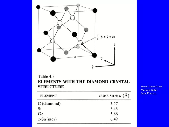
From Ashcroft and Mermin, Solid State Physics. NEMS: TOWARD PHONON COUNTING: Quantum Limit of Heat Flow. Roukes Group Cal Tech Tito. Biological Nanomotor. Gene chips, proteomics arrays. Silicon wafer fabrication. Taken from www.egg.or.jp/MSIL/english/index-e.html.

E N D
From Ashcroft and Mermin, Solid State Physics.
NEMS: TOWARD PHONON COUNTING: Quantum Limit of Heat Flow. Roukes Group Cal Tech Tito
Silicon wafer fabrication • Taken from www.egg.or.jp/MSIL/english/index-e.html
Silicon wafer fabrication – slicing and polishing • Taken from www.egg.or.jp/MSIL/english/index-e.html
Plasma Etchers Taken from http://www-bsac.EECS.Berkeley.EDU/~pister/245/
LPCVD Systems Taken from http://www-bsac.EECS.Berkeley.EDU/~pister/245/
Micromachining Ink Jet Nozzles Microtechnology group, TU Berlin
Bulk micromachined cavities Taken from http://www-bsac.EECS.Berkeley.EDU/~pister/245/ • Anisotropic KOH etch (Upperleft) • Isotropic plasma etch (upper right) • Isotropic BrF3 etch with compressive oxide still showing (lower right)
Deposit sacrificial layer Pattern contacts Deposit/pattern structural layer Etch sacrificial layer Surface Micromachining Taken from http://www-bsac.EECS.Berkeley.EDU/~pister/245/
Residual stress gradients Taken from http://www-bsac.EECS.Berkeley.EDU/~pister/245/ More tensile on top More compressive on top Just right! The bottom line: anneal poly between oxides with similar phosphorous content. ~1000C for ~60 seconds is enough.
Residual stress gradients Taken from http://www-bsac.EECS.Berkeley.EDU/~pister/245/ A bad day at MCNC (1996).
1 µm Scalloping and Footing issues of DRIE <100 nm silicon nanowire over >10 micron gap microgrid Footing at the bottom of device layer Milanovic et al, IEEE TED, Jan. 2001.
DRIE structures Taken from http://www-bsac.EECS.Berkeley.EDU/~pister/245/ • Increased capacitance for actuation and sensing • Low-stress structures • single-crystal Si only structural material • Highly stiff in vertical direction • isolation of motion to wafer plane • flat, robust structures Thermal Actuator Comb-drive Actuator 2DoF Electrostatic actuator
Sub-Micron Stereo Lithography New Micro Stereo Lithography for Freely Movable 3D Micro Structure -Super IH Process with Submicron Resolution- Koji Ikuta, Shoji Maruo, and Syunsuke Kojima Department of Micro System Engineering, school of Engineering, Nagoya University Furocho, Chikusa-ku, Nagonya 464-01, Japan Tel: +81 52 789 5024, Fax: +81 52 789 5027 E-mail: ikuta@mech.nagoya-u.ac.jp Fig. 6 Schematic diagram of the super IH process Fig. 1 Schematic diagram of IH Process Fig. 5 Process to make movable gear and shaft (a) conventional micro stereo lithography needs base layer (b) new super IH process needs no base Micro Electro Mechanical Systems Jan., 1998 Heidelberg, Germany
Sub-Micron Stereo Lithography New Micro Stereo Lithography for Freely Movable 3D Micro Structure -Super IH Process with Submicron Resolution- Koji Ikuta, Shoji Maruo, and Syunsuke Kojima Department of Micro System Engineering, school of Engineering, Nagoya University Furocho, Chikusa-ku, Nagonya 464-01, Japan Tel: +81 52 789 5024, Fax: +81 52 789 5027 E-mail: ikuta@mech.nagoya-u.ac.jp Fig. 10 Micro gear and shaft make of solidified polymer (b) side view of the gear of four teeth (d) side view of the gear of eight teeth Micro Electro Mechanical Systems Jan., 1998 Heidelberg, Germany
Takenfrom: http://www.imm-mainz.de/english/sk_a_tec/basic_te/liga.html