Download

1 / 26
300 likes | 847 Views
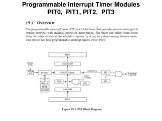
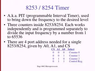
Programmable Interval Timer - 8254. 8254 Block Diagram. 8254 Control Word Format. Operating Modes. Mode 0 Interrupt on terminal count Mode 1 Programmable one shot Mode 2 Rate Generator Mode 3 Square wave rate Generator Mode 4 Software triggered strobe Mode 5 Hardware triggered strobe.

E N D
Operating Modes • Mode 0 Interrupt on terminal count • Mode 1 Programmable one shot • Mode 2 Rate Generator • Mode 3 Square wave rate Generator • Mode 4 Software triggered strobe • Mode 5 Hardware triggered strobe
Mode 4 Software triggered strobe Count value = 4In this mode after the count is loaded by the processor the count down starts. The output goes low for one clock period after the count down is complete. The count down can be suspended by making the GATE low .This is also called a software triggered strobe as the count down is initiated by a program.
Mode 5 Hardware triggered strobecount value = 5The count is loaded by the processor but the count down is initiated by the GATE pulse. The transition from low to high of the GATE pulse enables count down. The output goes low for one clock period after the count down is complete
Intel’s 8279 is a general purpose keyboard display controller that simultaneously drives the display of a system and interfaces a keyboard with the CPU, leaving it free for its routine task.
Architecture and Signal Descriptions of 8279 The keyboard display controller chip 8279 provides: a) a set of four scan lines and eight return lines for interfacing keyboards b) A set of eight output lines for interfacing display.
I/O Control and Data Buffers • The I/O control section controls the flow of data to/from the 8279. The data buffers interface the external bus of the system with internal bus of 8279. • The I/O section is enabled only if CS is low. The pins A0, RD and WR select the command, status or data read/write operations carried out by the CPU with 8279.
Control and Timing Register and Timing Control • These registers store the keyboard and display modes and other operating conditions programmed by CPU. The registers are written with A0=1 and WR=0. The Timing and control unit controls the basic timings for the operation of the circuit. Scan counter divide down the operating frequency of 8279 to derive scan keyboard and scan display frequencies.
Scan Counter The scan counter has two modes to scan the key matrix and refresh the display. In the encoded mode, the counter provides binary count that is to be externally decoded to provide the scan lines for keyboard and display (Four externally decoded scan lines may drive upto 16 displays). In the decode scan mode, the counter internally decodes the least significant 2 bits and provides a decoded 1 out of 4 scan on SL0-SL3( Four internally decoded scan lines may drive upto 4 displays). The keyboard and display both are in the same mode at a time.
Return Buffers and Keyboard Debounce and Control This section for a key closure row wise. If a key closer is detected, the keyboard debounce unit debounces the key entry (i.e. wait for 10 ms). After the debounceperiod, if the key continues to be detected. The code of key is directly transferred to the sensor RAM along with SHIFT and CONTROL key status.
Display Address Registers and Display RAM The display address register holds the address of the word currently being written or read by the CPU to or from the display RAM. The contents of the registers are automatically updated by 8279 to accept the next data entry by CPU.
Modes of Operation of 8279 The modes of operation of 8279 are as follows : 1. Input (Keyboard) modes. 2. Output (Display) modes.
Input ( Keyboard ) Modes : 8279 provides three input modes. These modes are as follows • Scanned Keyboard Mode • Scanned Sensor Matrix • Strobed input
Scanned Keyboard Mode : This mode allows a key matrix to be interfaced using either encoded or decoded scans. In encoded scan, an 8*8 keyboard or in decoded scan, a 4*8 keyboard can be interfaced. The code of key pressed with SHIFT and CONTROL status is stored into the FIFO RAM.
Scanned Sensor Matrix In this mode, a sensor array can be interfaced with 8279 using either encoded or decoded scans. With encoded scan 8*8 sensor matrix or with decoded scan 4*8 sensor matrix can be interfaced. The sensor codes are stored in the CPU addressable sensor RAM.
Strobed input In this mode, if the control lines goes low, the data on return lines, is stored in the FIFO byte by byte.