Download
1 / 22
220 likes | 397 Views
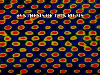
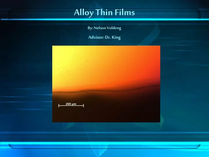
Alloy Thin Films By: Nelson Voldeng Advisor: Dr. King. Thin Film Applications. •Semiconductor processing for integrated electronic components and sensors •Super conductor materials for tomorrow’s new technologies •Anti-reflective (AR) optical films for better light transmission and clarity

E N D
Thin Film Applications • •Semiconductor processing for integrated electronic components and sensors • •Super conductor materials for tomorrow’s new technologies • •Anti-reflective (AR) optical films for better light transmission and clarity • •Clear conductive films used in touch-screen and plasma flat panel display technologies • •Hard film wear-ability coatings for tool steel and internal combustion engine components • •Reflective coatings for media storage like CD’s, DVD’s, and tape • •Conductive coatings for miniature medical probes and sensors • •Flexible and bendable lenses for X-ray wave length telescopes for space exploration • •Thin film coatings on Mylar, poly-carbine, and other substances for protective and/or decorative applications • Etc…
Overview of Research -Goals -Sputtered films/sectioned films -Taking data (largest hurdle) -Results -Future research
Goals • Research electronic applications (as well as others) for alloy thin films. • Have alloy film with columnar single crystals from top the film to bottom.
Physics Continued. • Em=0.4E*(M1+M2)/(M1+M2)^2 • E=Kinetic energy of incoming particle. • M1=Mass of incoming particle. • M2=Mass of target particle. • If Em>bond energy there’s a chance you can remove a target particle.
Hurdles with taking data • ZIESS and Profilometer microscope failed. AFM failed at first due to 150µm maximum scanning parameter. Succeeded by measuring cracks and scratches on films
Measuring the films at first • Not easy, time consuming, and poor data.
Results Overview • Height graphs for Ag and Cu • Approximate Deposition rates for Ag and Cu • Composition charts for CuAg film
Unusable height graph for Cu -Diamond scribe unreliable for scratching films. -Cuts into substrate and shatters film.
Most Recent Breakthrough! -Previously we thought Profilometry gave unusable results. -However, the once deemed useless profilometer is much quicker at measuring films. 1hr40mins per film (profilometer) vs. 5hrs per film (AFM)
For Future research • Film measurement Profilometer • Film sputtering scotch tape method, or lithography • Composition control Use targets with unequal element areas. Use target that is an alloy • Need more accurate results More data points for film thickness.
Thanks • Dr. King and the Materials Department. • Grad. Students and Kei.