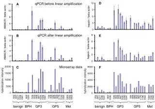
Download
1 / 8
80 likes | 89 Views
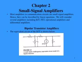
Chapter 13 Small-Signal Modeling and Linear Amplification. Microelectronic Circuit Design Richard C. Jaeger Travis N. Blalock. BJT Amplifier. BJT is biased in active region by dc voltage source V BE . Q-point is set at ( I C , V CE ) = (1.5 mA, 5 V) with I B = 15 m A.

E N D
Chapter 13Small-Signal Modeling and Linear Amplification Microelectronic Circuit Design Richard C. Jaeger Travis N. Blalock Microelectronic Circuit Design, 3E McGraw-Hill
BJT Amplifier BJT is biased in active region by dc voltage source VBE. Q-point is set at (IC, VCE) = (1.5 mA, 5 V) with IB = 15 mA. Total base-emitter voltage is: Collector-emitter voltage is: This is the load line equation. Microelectronic Circuit Design, 3E McGraw-Hill
BJT Amplifier (cont.) If changes in operating currents and voltages are small enough, then iC and vCE waveforms are undistorted replicas of input signal. Small voltage change at base causes large voltage change at collector. Voltage gain is given by: Minus sign indicates 1800 phase shift between input and output signals. 8 mV peak change in vBE gives 5 mA change in iB and 0.5 mA change in iC. 0.5 mA change in iC produces a 1.65 V change in vCE . Microelectronic Circuit Design, 3E McGraw-Hill
MOSFET Amplifier MOSFET is biased in active region by dc voltage source VGS. Q-point is set at (ID, VDS) = (1.56 mA, 4.8 V) with VGS = 3.5 V. Total gate-source voltage is: 1 V p-p change in vGS gives 1.25 mA p-p change in iD and 4 V p-p change in vDS. Microelectronic Circuit Design, 3E McGraw-Hill
Coupling and Bypass Capacitors C1 and C3 are large-valued coupling capacitors or dc blocking capacitors whose reactance at the signal frequency is designed to be negligible. C2 is a bypass capacitor that provides a low impedance path for ac current from emitter to ground, thereby removing RE (required for good Q-point stability) from the circuit when ac signals are considered. • AC coupling through capacitors is used to inject ac input signal and extract output signal without disturbing Q-point • Capacitors provide negligible impedance at frequencies of interest and provide open circuits at dc. Microelectronic Circuit Design, 3E McGraw-Hill
dc and ac Analysis • DC analysis: • Find dc equivalent circuit by replacing all capacitors by open circuits and inductors by short circuits. • Find Q-point from dc equivalent circuit by using appropriate large-signal transistor model. • AC analysis: • Find ac equivalent circuit by replacing all capacitors by short circuits, inductors by open circuits, dc voltage sources by ground connections and dc current sources by open circuits. • Replace transistor by small-signal model • Use small-signal ac equivalent to analyze ac characteristics of amplifier. • Combine end results of dc and ac analysis to yield total voltages and currents in the network. Microelectronic Circuit Design, 3E McGraw-Hill
dc Equivalent for BJT Amplifier • All capacitors in original amplifier circuits are replaced by open circuits, disconnecting vI , RI , and R3 from circuit. Microelectronic Circuit Design, 3E McGraw-Hill
ac Equivalent for BJT Amplifier Microelectronic Circuit Design, 3E McGraw-Hill