Download
1 / 32
330 likes | 506 Views
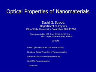
Magnificent Optical Properties of Noble Metal Spheres, Rods and Holes Peter Andersen and Kathy Rowlen Department of Chemistry and Biochemistry University of Colorado, Boulder Funded by the National Science Foundation. Enhanced Optical Processes from Nanometric Noble Metal Particles.

E N D
Magnificent Optical Properties of Noble Metal Spheres, Rods and Holes Peter Andersen and Kathy Rowlen Department of Chemistry and Biochemistry University of Colorado, Boulder Funded by the National Science Foundation
Enhanced Optical Processes from Nanometric Noble Metal Particles • 1970’s surface enhanced Raman scattering • 1980’s 106 enhancement of Raman scattering • 1980’s second harmonic generation • 1997 1014 enhancement of Raman scattering • 106 enhancement of fluorescence in nanorods • surface plasmon optics • Surface Plasmons: coherent oscillations of electron density at metal/dielectric interface
Enhanced Optical Transmission Ebbesen et al. “Extraordinary Optical Transmission Through Sub-Wavelength Hole Arrays” Nature, 1998, 391, 667-669
200 nm Ag film v.d. onto quartz • focused ion beam lithography • 150 nm holes • 600 nm to micron spacing Saloman et al. Phys. Rev. Lett. 2001, 86(6), 1110
Measured Near-Field Distribution Closest to simulated c (previous), hole d = 500 nm Thio et al., J. Opt. Soc. Am. B., 1999, 16(10), 1743
200 nm thick Ag • 150 nm holes • 900 nm spacing • Transmission efficiency = • fraction of light transmitted/ • fraction of surface area holes • = 2. • More than twice the light • that impinges on the holes is • transmitted through the film! Ebbesen et al. Nature 1998, 391,667
Hole spacing determines peak position • Peak position independent of hole d • Independent of metal (Ag, Cr, Au) • Must be metal (Ge doesn’t work) Ebbesen et al. Nature 1998, 391,667
T scales with d2, independent of versus (d/ )4 for Bethe sub- aperture =500 nm
Enhancement / Transport Mechanism? Not cavity resonance since peak position (in spectrum) does not significantly depend on hole dimensions Not waveguiding because film thickness too small (200 nm) Surface plasmon tunneling? Surface plasmon scattering?
For a surface that can support a surface plasmon, • the wave vector, ksp is: • The difference between the in-plane wave vector of light, ki, and the surface plasmon wave vector, ksp, can be compensated for by diffraction on periodic surface structure:
Ag Ag/Ni Ni Grupp et al., Appl. Phys. Lett. 2000, 77(11), 1569
Transmission relatively independent of wall metal Grupp et al., Appl. Phys. Lett. 2000, 77(11), 1569
Further evidence for surface plasmon involvement Sonnichsen et al., Appl. Phys. Lett. 2000, 76(2), 140
Left: Calculated near-field transmission intensity [(c) = 300 d, 900 nm a, 800 nm ] Calculated intensity enhancement near hole edge ~ 500x 15 nm above 100 nm above Saloman et al. Phys. Rev. Lett. 2001, 86(6), 1110
Surface Plasmon Activated Devices Thio et al., Physica B, 2000, 279, 90
Transmission through single hole with array of dimples Single hole in smooth surface Grupp et al. Adv. Matr. 1999, 11(10), 860
For coherent 670 nm light T is 60x greater than typical NSOM tapered fiber with 200 nm aperture Thio, Lezec, Ebbesen Physica B, 2000, 279, 90
Applications, Applications, Applications! Reflection mode? SERS at edges? Field in channel?
Surface Plasmon Optics: • use SP’s for manipulation of optical fields • SP lenses, mirrors and flashlights • (e.g., Smolynaninov et al. Phys. Rev. B. 1997, 56(3) 1601-1611.)
Optical Enhancement via Surface Plasmon Coupling Surface plasmon lense Light harvesting indentations Field enhanced detection region hn Surface plasmon mirror Transmission channel
Si substrate Electron-Beam Nanolithography (Peter Andersen) Spin coat substrate with PMMA resist Expose to electron beam Develop in MIBK/IPA Metalize by vapor deposition
Grating Constant (ao) target ao 450 nm measured ao 450 nm
Photolithography (Michele Jacobson) Lens Au Mirror Pinhole Nd:YAG Laser = / 2sin