Download
1 / 22
220 likes | 401 Views
Chapter 4. MOS Systems. Total 3 hours. The Adventure of Carriers.

E N D
Chapter 4. MOS Systems Total 3 hours.
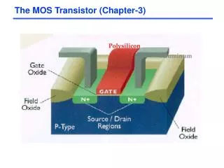
The Adventure of Carriers The description must now borrow a picture from the classical books of adventure. To place a negative electrode against a semiconductor with negative carriers - this is like bringing a ship up to a quay in the Orient, with the yellow flag of the plague hoisted. The place becomes deserted by its carriers. Unloading - current - is blocked. But exchange that negative flag of pestilence for a positive sign and the carriers will return, the contact becoming conducting. Electrically this is called rectification. In those seafaring tales it was perhaps possible to induce the carriers to return, without striking the flag, merely by throwing some gold coins on the quay, thus positively destroying the insulation. It is possible to destroy the blockade in the semiconductor in a similar fashion by throwing in some positive holes around which the negative carriers will gather. This is transistor action. It is a fine thing that the carriers' strike can be broken up by rather few holes, which do not cost much energy.
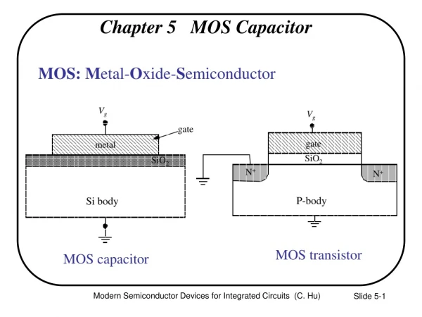
Equilibrium Band Diagram Equilibrium implies the existence of a path for charge flow between the metal and the silicon other than the oxide. But a barrier for electron flow along both directions
Voltage Drop across Oxide • Depends upon specific oxide properties.
Capacitance • Accumulation: Determined by oxide • Flat band: Debye length (no surface potential) • Depletion: Width of the surface depletion layer • Inversion • Low frequency: Inversion layer population can follow • High frequency: Inversion layer cannot respond; charge modulated by the movement of carriers at the far edge of the depletion layer • Deep depletion: Inversion layer cannot form at all
Charge in Oxide Flat band
Charge-Coupled Devices • How is an image stored digitally? • How to acquire an image? What are the basic principles of charge-coupled devices (CCDs)? pixels, or picture elements
Charge-Coupled Device CCDs consist of almost entirely close spaced array of MOS capacitors. In a MOS capacitor, the electrical signal is represented by the channel (inversion layer) charge, which can be transferred to the channel region of the adjacent device.
The nine-stage CCD illustrates how information is transferred from left to right, by changing gate voltages.