Download

1 / 34
340 likes | 512 Views
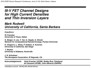
2010 IEEE Device Research Conference, June 21-23, Notre Dame, Indiana. III-V FET Channel Designs for High Current Densities and Thin Inversion Layers. Mark Rodwell University of California, Santa Barbara. Coauthors: W. Frensley: University of Texas, Dallas

E N D
2010 IEEE Device Research Conference, June 21-23, Notre Dame, Indiana III-V FET Channel Designs for High Current Densities and Thin Inversion Layers Mark Rodwell University of California, Santa Barbara Coauthors: W. Frensley: University of Texas, Dallas S. Steiger, S. Lee, Y. Tan, G. Hegde, G. KlimekNetwork for Computational Nanotechnology, Purdue University E. Chagarov, L. Wang, P. Asbeck, A. Kummel, University of California, San Diego T. BoykinUniversity of Alabama, HuntsvilleJ. N. SchulmanThe Aerospace Corporation, El Segundo, CA. Acknowledgements: Herb Kroemer (UCSB), Bobby Brar (Teledyne) Art Gossard (UCSB), John Albrecht (DARPA) rodwell@ece.ucsb.edu 805-893-3244, 805-893-5705 fax
Thin, high current density III-V FET channels InGaAs, InAs FETs THz & VLSI need high current low m*→ high velocities FET scaling for speed requires increased charge density low m* →low charge density Density of states bottleneck (Solomon & Laux IEDM 2001) → For < 0.6 nm EOT, silicon beats III-Vs Open the bottle ! low transport mass → high vcarriermultiple valleys or anistropic valleys → high DOSUse the L valleys.
Goal: double transistor bandwidth when used in any circuit → reduce 2:1 all capacitances and all transport delays→ keep constant all resistances, voltages, currents Simple FET Scaling gate-source, gate-drain fringing capacitances: 0.15-0.25 fF/mm must increase gate capacitance/area must reduce gate length
FET Scaling Laws Changes required to double device / circuit bandwidth. laws in constant-voltage limit: Current densities should doubleCharge densities must double
Calculating Current: Ballistic Limit Do we get highest current with high or low mass ?
Drive current versus mass, # valleys, and EOT InGaAs MOSFETs: superior Id to Si at large EOT.InGaAs MOSFETs: inferior Id to Si at small EOT. Solomon / Laux Density-of-States-Bottleneck → III-V loses to Si.
Transit delay versus mass, # valleys, and EOT Low m* gives lowest transit time, lowest Cgs at any EOT.
Low effective mass also impairs vertical scaling Shallow electron distribution needed for high Id, high gm / Gds ratio, low drain-induced barrier lowering. Energy of Lth well state For thin wells, only 1st state can be populated. For very thin wells, 1st state approaches L-valley. Only one vertical state in well. Minimum ~ 3 nm well thickness. → Hard to scale below 10-16 nm Lg.
Standard III-V FET: G valley in [100] orientation 3 nm GaAs wellAlSb barriers G=0 eVL=177 meVX[100]= 264 meVX[010] = 337 meV
1st Approach: Use both G and L valleys in [111] 2.3 nm GaAs wellAlSb barriers[111] orientation G= 41 meVL[111] (1)= 0 meVL[111] (2)= 84 meVL[111] , etc. =175 meVX=288 meV
Combined G-L wells in {111} orientation vs. Si combined (G -L) transport 2 nm GaAs G /L well→ g =2, m*/m0=0.07 4 nm GaSb G /L well→ mG*/m0=0.039, mL,t*/m0=0.1
2nd Approach: Use L valleys in Stacked Wells Three 0.66 nm GaAs wells0.66 nm AlSb barriers [111] orientation L[111](1) = 0 meVL[111](2)= 61 meVL[111](3)= 99 meV G=338 meVL[111], etc =232 meVX=284 meV
Concerns Nonparabolic bands reduce bound state energies Failure of effective mass approximation:1-2 nm wells 1-2 monolayer fluctuations in growth → scattering→ collapse in mobility
Steiger, Klimeck, BoykinRyu, Lee, Hegde, Tan Purdue Confirmation
1-D FET array = 2-D FET with high transverse mass 2-D FET 1-D Array FET Weak coupling → narrow transverse-mode energy distribution→ high density of states
4th Approach: {110} Orientation→ Anisotropic Bands transport
Anisotropic bands, e.g. {110} Transport in {110} oriented L valleys
Scaled FET performance: fixed vs. increasing DOS fmax ft SCFL divider speed mA/mm→ VLSI metric Increased density of states needed for high drive current, fast logic @ 16, 11, 8 nm nodes
10 nm / 3 THz III-V FETs: Challenges & Solutions gate dielectric:decrease EOT 2:1 To double the bandwidth: channel: keep same velocity, butthin channel 2:1increase density of states 2:1 S/D access regions:decrease resistivity 2:1 S/D regrowth Wistey et alSingisetti et al