Download
1 / 18
180 likes | 363 Views
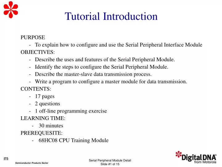
Tutorial Introduction. PURPOSE - To explain how to configure and use the Serial Peripheral Interface Module OBJECTIVES: - Describe the uses and features of the Serial Peripheral Module. - Identify the steps to configure the Serial Peripheral Module.

E N D
Tutorial Introduction PURPOSE - To explain how to configure and use the Serial Peripheral Interface Module OBJECTIVES: - Describe the uses and features of the Serial Peripheral Module. - Identify the steps to configure the Serial Peripheral Module. - Describe the master-slave data transmission process. - Write a program to configure a master module for data transmission. CONTENTS: - 17 pages - 2 questions - 1 off-line programming exercise LEARNING TIME: • 30 minutes PREREQUESITE: • 68HC08 CPU Training Module
SPI Uses and Features • Full-duplex synchronous serial operation • Smaller packages • Lower cost • Maximum master mode frequency = bus frequency / 2 • Maximum slave mode frequency = bus frequency • Serial clock with programmable polarity and phase • Two separately enabled interrupts: • SPRF (SPI Receiver Full) • SPTE (SPI Transmitter Empty)
Master-Slave Overview TRANSMIT DATA REGISTER TRANSMIT DATA REGISTER RECIVE DATA REGISTER RECIVE DATA REGISTER PIN CONTROL LOGIC M CLOCK LOGIC S SS Slave MCU Master MCU INTERNAL BUS INTERNAL BUS SHIFT REGISTER MISO SHIFT REGISTER x x x x x x x x x x x x x x x x MOSI SPSCK SPRIE SPTIE 0 0 SS VDD SPRF SPTE 0 1 0 1
Master-Slave Connections SS SS VDD MASTER MCU SLAVE MCU MISO MISO SHIFT REGISTER MOSI MOSI SHIFT REGISTER SPSCK SPSCK BAUD RATE GENERATOR
SPI Control Register (SPCR) SPRIE - SPI Interrupt Enable Bit 1 - SPRF CPU interrupt requests enabled 0 - SPRF CPU interrupt requests disabled
SPI Control Register (SPCR) SPRIE - SPI Interrupt Enable Bit 1 - SPRF CPU interrupt requests enabled 0 - SPRF CPU interrupt requests disabled
SPI Status and Control Register (SPSCR) Display bit annotation here.
Master-Slave Initialization StepControl Bits 1) Initialize SPI clock frequency. SPR1 and SPR0 in SPSCR 2) Configure the clock. CPOL and CPHA in SPSCR 3) Select master/slave mode. SPMSTR in SPCR 4) Enable interrupts if desired. SPTIE and SPRIE in SPCR 5) Enable master SPI. SPE in SPCR 6) Enable slave SPIs. SPE in SPCR
Data Transmission Example TRANSMIT DATA REGISTER TRANSMIT DATA REGISTER SHIFT REGISTER 1 0 1 0 1 0 1 0 RECIVE DATA REGISTER RECIVE DATA REGISTER PIN CONTROL LOGIC MOSI M CLOCK LOGIC S 1 0 1 0 1 0 1 0 SS Slave MCU Master MCU INTERNAL BUS INTERNAL BUS 1 0 1 0 1 0 1 0 1 0 1 0 1 0 1 0 SHIFT REGISTER MISO SHIFT REGISTER x x x x x x x x x x x x x x x x MOSI SPSCK SPRIE SPTIE 0 0 SS VDD SPRF SPTE 1 0 0 1
1 2 3 4 5 6 7 8 MSB BIT 6 BIT 5 BIT 4 BIT 3 BIT 2 BIT 1 LSB MSB BIT 6 BIT 5 BIT 4 BIT 3 BIT 2 BIT 1 LSB Transmission Formats (CPH = 0) SPSCK cycle # from reference SPSCK; CPOL = 0 SPSCK; CPOL =1 MOSI from master MISO from slave SS; to slave Capture strobe
1 2 3 4 5 6 7 8 MSB MSB BIT 6 BIT 6 BIT 5 BIT 5 BIT 4 BIT 4 BIT 3 BIT 3 BIT 2 BIT 2 BIT 1 BIT 1 LSB LSB MSB MSB BIT 6 BIT 6 BIT 5 BIT 5 BIT 4 BIT 4 BIT 3 BIT 3 BIT 2 BIT 2 BIT 1 BIT 1 LSB LSB Transmission Formats (CPH = 1) SPSCK cycle # from reference SPSCK; CPOL = 0 SPSCK; CPOL =1 MOSI from master MISO from slave SS; to slave Capture strobe
Question With the bus frequency set to 16 Mhz and the SPI baud rate select bits set to 10, what is the master SPI baud rate? a) 0.25 MHz b) 1 MHz c) 2 MHz d) 4 MHz
Question What happens when the master SPI attempts to send another byte to the slave SPI, when the slave SPI receive data register contains a byte of data previously transmitted but not yet read by the slave CPU? Click on your choice. a) No transmission occurs b) All 8-bits are transfered from the master’s shift register to the slave’s shift register, while data in the slave’s receive data register is overwritten. c) All 8-bits transferred from the master’s shift register to the slave’s shift register, while data in the slave’s receive data register is not overwritten until the CPU first reads the slave’s receive data register.
Programming Exercise • Configure a non-interrupt driven master. • Transmit the value $55. • Use a serial-in/parallel-out, 8-bit shift register: • Register is chip-selected with the port PB3 line at a low voltage level. • Verify that the PB3 line is high between transfers. • Configure the SPI clock: • Idle low and take data on rising clock edges. • SPI clock frequency < 300 kHz. • Assume system clock frequency of 8 MHz.
SPI Exercise Solution PTB EQU $01 ; Port B Data register DDRB EQU $05 ; Port B Data Direction register SPCR EQU $10 ; SPI Control register SPSCR EQU $11 ; SPI Status and Control register SPDR EQU $12 ; SPI Data (Read=rcv, Write=xmt) ; ; Select Port B inputs/outputs & levels: ; BSET #3,PTB ; Make PB3 output value high BSET #3,DDRB ; Make PB3 an output LDA #$06 ; Load accumulator (ACC) with: ; " MOSI & SPSCK = outputs" value ; " MISO & SS* = inputs" value STA DDRF ; Store ACC to DDRF register ; ; Select master mode, clock, and enable SPI: LDA #$02 ; Load ACC with value that selects 300 kHz STA SPSCR ; Store ACC to SPSCR LDA #$22 ; Load ACC with value to configure SPSCR STA SPCR ; Store ACC to SPCR ; ; Send $55 to shift register: ; BCLR #3,PORTB ; Make PB3 output low (chip-select register) LDA #$55 ; Load ACC with $55 STA SPDR ; Store ACC to SPDR WAIT BRCLR #7,SPSCR,WAIT ; Wait until transmission is complete BSET #3,PORTB ; Make PB3 output high (deselect register) DONE BRA DONE ; Done, stay here
Tutorial Completion • - SPI Uses and Features • - SPI Configuration • - SPI Master-Slave Data Transmission