Download
1 / 15
150 likes | 691 Views
Development of Slurries for Polishing SiLK TM -Integrated Wafers. Dr. David Merricks IITC 2003. Acknowledgements to Bob Her, David Tysiac, Sheldon Mao, Lynn Murray of Ferro Electronic Material Systems and Ketan Itchaporia, Michael Simmonds of Dow Chemical. Outline.

E N D
Development of Slurries for Polishing SiLKTM-Integrated Wafers Dr. David Merricks IITC 2003 Acknowledgements to Bob Her, David Tysiac, Sheldon Mao, Lynn Murray of Ferro Electronic Material Systems and Ketan Itchaporia, Michael Simmonds of Dow Chemical
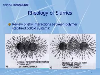
Outline • Introduction to SiLKTM Integrated Wafers • Polishing Approaches • Polishing Studies • Material Selectivities and Removal Rates • Polishing - Stopping on SiLKTM • Polishing - Stopping on SiCN • CMP-Stop Evaluation • Planarization Efficiency • Ferro Slurries • Tizox SRS-908 Copper Slurry • Tizox SRS-876 Damascene Slurry • Future Work
SiLKTM-Integrated Wafers Copper (1um EP Cu + 100nm seed) Barrier layer (25nm Ta) Top hardmask (200nm SiO2) Lower hardmask SiCN 100nm Dielectric (520nm SiLK) Si wafer (high conductivity) Objective - develop slurries and polishing processes compatible with the materials used in SiLKTM/Ensemble integrated stacks Ensemble Spin-on Stack CMP-1 Wafers CMP-2 Wafers Copper (1um electroplated + 100nm seed) Barrier layer (25nm Ta) Top hardmask (0-100nm SiO2) Lower hardmask (100nm SiCN) Dielectric (520nm SiLK) Copper diffusion passivation layer (50nm SiCN) Isolation layer (550nm SiO2) Si wafer
2-Slurry Polishing Process • A 2-slurry polishing scheme is favored, to minimize dishing/erosion 2nd step 1st step SiCN/SiLK/Si or Cu/Ta/TEOS/SiCN/SiLK/Si SiLK/Si • The initial development work was carried out on a Strasbaugh 6EC • rotary tool. CMP-1 and CMP-2 wafers were polished on the Applied • Materials Mirra tool • IC1000/Suba IV pads were used throughout
Material Selectivities • Slurries have been developed which give both low- and • high-selectivity across the various materials found in the CMP-1 • and CMP-2 integrated stack. Examples are shown below. • Copper slurry removal rates; • Cu Cu %WIWNU Ta TaN • Slurry IA 5500-6500 3-5 <50 <50 • Slurry IB 5000-6000 3-5 195 262 • Damascene slurry removal rates • Cu Ta TaNTEOS SiLKTM • Slurry IIA 570(1) 711(1.25) 689(1.21) 917(1.61) 569(1) • Slurry IIIA 147(1) 519(3.53) 753(5.12) 56(0.38) --- • Rms surface roughness of post-polished SiLKTM is typically <3 Angstroms • and %WIWNU is <3%.
SiLKTM Removal Rate SiLK RR vs PSI Downforce Pressure 850.0 5 750.0 4 Removal Rate (A/min) y = 71.854x + 429.55 2 R = 0.9617 650.0 3 2 550.0 1 2 3 4 5 6 Downforce (psi) • Slurry used here is IIA • Strasbaugh 6EC polishing tool
Polishing - Stopping on SiLKTM • Slurries have been developed for direct polishing on SiLKTM. • FTIR spectroscopic analysis carried out at Dow, Midland has • shown that these slurries do not lead to any oxidation of the • dielectric surface and therefore no change in dielectric constant • A modified edge lift-off (m-ELT) technique has shown there is • no delamination or peeling of SiLKTM under the processing • downforces used (2-3psi) • In low-selectivity schemes, the SiLKTM RR should closely match • the RRs of copper and barrier • Cu Ta TaN TEOSSiLKTM • Slurry IIA 570(1) 711(1.25) 689(1.21) 917(1.61) 569(1) • Slurry IIB 818(1) 755(0.92) 892(1.09) 850(1.04) 813(0.99) • Slurry IIC 361(1) 684(1.89) 888(2.45) 903(2.5) 868(2.4)
Polishing - Stopping on SiLKTM • The selectivities are easily ‘tunable’ by the choice of additives • Damascene slurries have been developed that lead to a very low • RR for SiLKTM (polishing can stop on SiLKTM); • Cu Ta TaN TEOS SiLKTM • Slurry IID 500(1) 780(1.56) 861(1.72) 755(1.51) <50 • ….or give a very high SiLKTM RR relative to other materials in • the stack; • Cu Ta TaN TEOSSiNSiLKTM • Slurry IIE 133(1) 97(0.73) 258(1.94) 204(1.53) 152(1.14) 2903(21.82) • RRs are in A/min, polished at 3psi/60rpm/200ml-min flow rate
Polishing - Stopping on SiCN • Ideally, the CMP consumables should never come into contact with • the SiLKTM material • Hardmask materials are integrated to protect the soft low-modulus • materials during CMP • SiCN (k=4.9) is used as CMP-stop in CMP-1 and CMP-2 wafers • However, using many slurries (i.e. slurry IIA) the RR of SiCN is high • A new slurry (IIIA) was developed which gives very low SiCN removal • This slurry has been used along with the copper slurry IB in a 2-slurry • polishing scheme for CMP-1 wafers, stopping on SiCN • Removal rates (A/min) for IIA and IIIA are shown below (2psi/60rpm); • SiCNTEOS • Slurry IIA 69 2365 • Slurry IIIA 956 602 • Work continues on evaluating additives for further selectivity optimization
Polishing - Stopping on SiCN 2 • Polishing on the AMAT Mirra tool has shown that it is possible to • use a non-selective Damascene slurry with CMP-1 wafers and stop • on SiCN using optical endpoint detection • The trace for slurries IB and IIA is shown below;
CMP-Stop Comparison Slurry IIIA Slurry IIA Slurry IVA • Several slurries have been evaluated with alternative CMP-stop materials • such as SiC and Ensemble CS (organosilicate, k=2.9) • SiC and SiCN showed similar polishing characteristics, but Ensemble CS • gave relatively high RRs from all slurries - more work is necessary
CMP-2 - Planarization Evolution of feature 9_1 step height 8000 6000 Step height, Angstroms 4000 2000 0 0 100 200 300 Polish time, sec • A 2-slurry process was used to measure step-height reduction • across a CMP-2 wafer (in this case on 90% dense features) • Here, the second slurry was introduced after 80 seconds
Ferro Slurries for Cu/Low-k Polishing Copper Slurry: Tizox SRS-908 • Formulated to remove the bulk of the copper overplate • RR of copper in the 5000-6500 A/min range using • moderate to low range of downforce pressures and • platen speeds • Very low defectivity/pitting observed • RMS surface roughness - 10-15 Angstroms • Long shelf (oxidizer is separated) • Effective with downforce pressures compatible with • low-k dielectric integration
Ferro Slurries for Cu/Low-k Polishing Damascene Slurry: Tizox SRS-876 • Formulated to remove residual copper and barrier layer • Close match of Cu/Ta/TaN/TEOS/SiLKTM RRs • RRs/selectivity (at 3psi/60rpm) for Cu:Ta:TaN:TEOS:SiLKTM; • 818(1):755(0.92):892(1.09):850(1.04):813(0.99) • RRs can be tuned in the 500-900 A/min range • Selectivities can be tuned by choice of additives • No copper pitting or corrosion • Effective with low and moderate downforce processes compatible • with low-k dielectric integration - no adhesion failure • Slurries are compatible with SiLKTM low-k dielectric materials • - no change in dielectric constant
Future Work • A new cleanroom facility (5000 sq.ft - 2500 sq.ft of class 10 area) • at FEMS Penn Yan, NY has been qualified and is scheduled to be • operational by the end of June • Future SiLKnet work will be carried out in this facility on the • Applied Materials Mirra tool • Slurries and processes for polishing CMP-1 and CMP-2 wafers • containing porous SiLKTM (and SiLK-D when available) • will be developed • Both high- and low- selectivity slurry formulations will continue • to be developed • A link to the Ferro SiLKnet work can be found on the SiLKnet • website and also on; • www.ferro.com/ourproducts/electronic/knowledgebase.htm