Download
1 / 3
30 likes | 67 Views
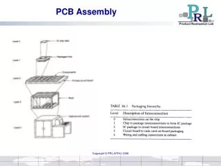
While designing the PCB boards Assembly, there are three main areas designers need to pay attention for better and faster PCBs.

E N D
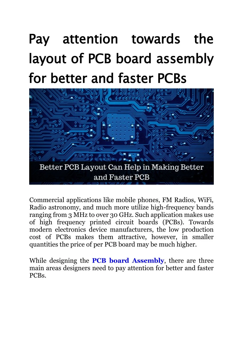
Pay atte layout of PCB board assembly for better and faster Pay attention towards the layout of PCB board assembly for better and faster PCBs ntion towards the PCBs Commercial applications like mobile phones, FM Radios, WiFi, Radio astronomy, and much more utilize high-frequency bands ranging from 3 MHz to over 30 GHz. Such application makes use of high frequency printed circuit boards (PCBs). Towards modern electronics device manufacturers, the low production cost of PCBs makes them attractive, however, in smaller quantities the price of per PCB board may be much higher. While designing the PCB board Assembly, there are three main areas designers need to pay attention for better and faster PCBs.
Construction Materials Designers in the process of designing PCB board’s assembly, mainly consider two significant characteristics the dielectric constant and loss tangent of the PCB material. The speed at which signals travel through the board gets affected by the dielectric constant, whereas, the loss tangent refers to the amount of sign loss by absorption within the material. For those using frequencies over 1 GHz, FR4 is a standard material for constructing low-frequency circuits, and there is a requirement of more premium materials. Construction Materials Component Interaction To consider points of connection between components and the PCB board assembly is essential for designers of high-frequency boards. For instance, placement of a pad over a ground plane may act as a capacitor. As surface mount devices (SMD) have small constructional features and lead length the use of this device solves the query to a large extent. With the rise in the frequency, passive components which include those in SMD form may feature non-ideal characteristics. Component Interaction Layout of An individual must target achieving high-speed operations in a low-power environment once the designer has satisfactorily concluded the choice of construction material and the components that include, reducing any ground bounce effects, proper signal line termination, impedance matching, minimizing onboard noise generation, and cross-talk between traces. Layout of Traces Traces In minimizing onboard noise generation, its two significant aspects distribution of power throughout the board and power
noise filtering with which the amount of noise generated on- board can get lessen. Designers might either use power planes or bus network for distributing power throughout the PCB board assembly. Generally, power plans on a multi-layer PCB consist of two or more metal layers carrying GND and Vcc to the devices. Moreover, a power plane nearly covers the full area of the PCB, DC resistance of such spheres is low and thus keeps the Vcc level constant while distributing it equally to all devices. Additionally, the signal which PCB carries also provide the very high current- sink capability, proper shielding for the signs and noise protection. Hence, for making it work as intended at high frequencies, there is a lot a designer can do with a better PCB layout, apart from selecting the suitable high-frequency material. The PCB board assembly is custom designed, as each of them is unique and the software package which offers a wide range of features helps the designers by using a PCB CAD or design suite software. PCC — One stop solution for PCB engineering, design, CCA and testing has experienced PCB designers who help in the successful delivery of effective electrical designs. EE engineers do our designs with 25 years of product design experience. We design per IPC class II or Class III or to any given specifications. Our PCB designers have proven expertise in developing a physical layout for completed schematic designs. Moreover, PCC specializes in rapid PCB Manufacturing Services (EMS). assembly and Electronic