Download
1 / 47
490 likes | 786 Views
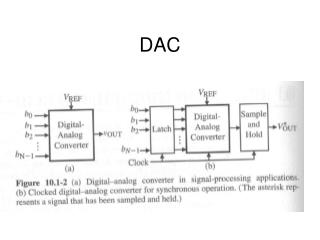
41 st DAC Tuesday Keynote. Giga-scale Integration for Tera-Ops Performance Opportunities and New Frontiers. Pat Gelsinger Senior Vice President & CTO Intel Corporation June 8, 2004. Litho Cost. FAB Cost. Test Capital. G. Moore ISSCC 03. www.icknowledge.com. Based on SIA roadmap.

E N D
Giga-scaleIntegration for Tera-OpsPerformanceOpportunities and New Frontiers Pat Gelsinger Senior Vice President & CTO Intel Corporation June 8, 2004
Litho Cost FAB Cost Test Capital G. Moore ISSCC 03 www.icknowledge.com Based on SIA roadmap Why Bother?
Litho Cost FAB Cost Scaling dead at 130-nm, says IBM technologistBy Peter Clarke , Silicon Strategies May 04, 2004 (2:28 PM EDT)PRAGUE, Czech Republic — The traditional scaling of semiconductor manufacturing processes died somewhere between the 130- and 90-nanometer nodes, Bernie Meyerson, IBM's chief technology officer, told an industry forum. G. Moore ISSCC 03 www.icknowledge.com Why Bother?
$ per MIPS $ per Transistor No exponential is forever, but you can delay forever… –Gordon Moore Believe in the Law
Moore’s Law Is Alive & Well … CMOS Outlook However …
Guiding Observations Transistors (and silicon) are free Power is the only real limiter Optimizing for frequency AND/OR area may achieve neither
GATE DRAIN SOURCE BODY MOS Transistor Scaling GATE Xj DRAIN SOURCE Tox D BODY Leff Technology has scaled well, and will continue…
Delivering Performance in Power Envelope Mobile, Power Envelope ~20-30W Desktop, Power Envelope ~60-90W Server, Power Envelope ~100-130W
G G Strained Silicon – 90nm+ S D S D NMOS PMOS Tensile Si3N4 Cap SiGe S-D creates strain 10-25% higher ON current 84-97% leakage current reduction OR 15% active power reduction Source: Mark Bohr, Intel
90nm MOS Transistor 50nm Gate Gate Leakage Solutions: High-K + Metal Gate 1.2 nm SiO2 Silicon substrate Gate & Source-Drain Leakage
Gate 3 Drain Lg WSi Gate 1 TSi Source Gate 2 New Transistors: Tri-Gate… Tri-gate Gate Drain Source Source: Intel Improved short-channel effects Higher ON current for lower SD Leakage Manufacturing control: research underway
Metal Interconnects Interconnect RC Delay
Uniform Non-uniform Random Dopant Fluctuations
Sub-wavelength Lithography Adds Variations Lithography Wavelength 365nm 248nm 193nm 180nm 130nm Gap 90nm 65nm Generation 45nm 32nm 13nm EUV
Impact of Static Variations 1.4 Frequency ~30% Leakage Power ~5-10X 30% 1.3 1.2 130nm Normalized Frequency 1.1 1.0 5X 0.9 1 2 3 4 5 Normalized Leakage (Isb)
Dynamic Variations: Vdd & Temperature Temperature Variation (°C) Hot spots Heat Flux (W/cm2) Results in Vcc variation
Technology Challenges Power: Active + Leakage Interconnects (RC Delay) Variations
Active Power Reduction High Supply Voltage Slow Fast Slow Multiple Vdd Low Supply Voltage • Vdd scaling will slow down • Mimic Vdd scaling with multiple Vdd • Challenges: • Interface between low & high Vdd • Delivery and distribution
Body Bias Stack Effect Sleep Transistor Vbp Vdd +Ve Logic Block Equal Loading Vbn -Ve 2-10X Reduction 5-10X Reduction 2-1000X Reduction Leakage Control
Adaptive Body Biasing too leaky ABB Number of dies Number of dies too slow RBB RBB FBB FBB f f f f target target Frequency Frequency
No BB ABB Within die ABB 97% highest bin 100% yield 100% yield with Adaptive Body Biasing 97% highest freq bin with ABB for within die variability Adaptive Body Biasing 100% 60% Accepted Die 20% 0% Low Frequency Bin High Frequency Bin
Vdd/2 Vdd Freq = 1 Vdd = 1 Throughput = 1 Power = 1 Area = 1 Power Den = 1 Freq = 0.5 Vdd = 0.5 Throughput = 1 Power = 0.25 Area = 2 Power Den = 0.125 Logic Block Logic Block Logic Block RC Delay Tolerant Design Lower Power And Power Density RC Delay Mitigation Throughput Oriented Design
power 2 2 target frequency probability 1.5 1.5 1 1 0.5 0.5 0 0 large high small low Transistor size Low-Vt usage Variation Tolerant Circuit Design • Higher probability of target frequency with: • Larger transistor sizes • Higher Low-Vt usage • But with power penalty
60% # critical paths 1.4 40% 1.3 Number of dies 20% Mean clock frequency 1.2 0% 0.9 1.1 1.3 1.5 Clock frequency 1.1 1 9 17 25 # of critical paths NMOS Device I 40% ON PMOS 20% 1.0 # of samples (%) Delay to Ion-s 40% 0.5 20% Ratio of 0% delay-s -16% -8% 0% 8% 16% 0.0 16 49 Variation (%) Logic depth Variations and µ-architecture
1.5 1 0.5 0 More Less # uArch critical paths frequency target frequency probability Variation Tolerant µ-architecture 1.5 1 0.5 0 Small Large Logic depth • Decrease variability in the design: • Deeper logic depth • Smaller number of critical paths
Implications For CAD Logic & Circuits Layout Test
Path Delay Deterministic Deterministic Probabilistic Frequency Probabilistic 10X variation ~50% total power # of Paths # of Paths Delay Target Delay Target Leakage Power Probabilistic Design Due to variations in: Vdd, Vt, and Temp Probability Delay Deterministic design techniques inadequate in the future
Today: Local Optimization Single Variable Tomorrow: Global Optimization Multi-variate Shift in Design Paradigm • Multi-variable design optimization for: • Yield and bin splits • Parameter variations • Active and leakage power • Performance
Vdd Vdd Ip Op Op Vss Vss Today’s Freelance Layout No layout restrictions
Vdd Vdd Ip Op Op Vss Vss Future Transistor Orientation Restrictions Transistor orientation restricted to improve manufacturing control
Future Transistor Width Quantization Vdd Vdd Op Ip Op Vss Vss
Today’s Metric: Maximizing Transistor Density Dense layout causes hot-spots
Tomorrow’s Metric: Optimizing Transistor & Power Density Balanced Layout
Other Challenges … Test & Debug
Understandable … Test Capital/ Transistor Test Capital Based on SIA roadmap Based on SIA roadmap Disturbing … Test Challenges
0.25 >1E-4 0.4 On-Die Scope Waveform 0.125 1E-5 0.2 Differential Voltage (V) 0.0 Voltage (V) 0 1E-6 -0.2 -0.4 0.0 1.8 3.6 5.4 7.1 8.9 10.7 12.5 1E-7 -0.125 Time (ns) <1E-8 -0.25 0 104 208 312 416 Time (ps) On Die Test Methodology On die debug & test of 8Gb/sec IO interface • Move from external to on-die “self testing” • High-speed test & debug hardware on each die • Low speed, low cost, interface to external tester ISSCC 2003: 8Gb/s Differential Simultaneous Bidirectional Link with 4mV, 9ps Waveform Capture Diagnostic Capability
Other Challenges … Mixed-signal Design System-level Design Correctness Multi-clock domains Resiliency
Summary BELIEVE CMOS scaling will continue, transistors become free SHIFT Deterministic Probabilistic, Single Multi EMBRACE local to global optimization: power,…