Download
1 / 54
580 likes | 1.24k Views
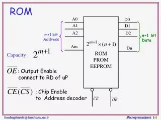
: Output Enable connect to RD of uP. ROM. A0. D0. A1. D1. A2. D2. m+1 bit Address. n+1 bit Data. Am. Dn. ROM PROM EEPROM. Capacity :. : Chip Enable to Address decoder. Timing Diagram for a Typical ROM. A0-Am. D0-Dn. OE falls to data valid.

E N D
: Output Enable connect to RD of uP ROM A0 D0 A1 D1 A2 D2 m+1 bit Address n+1 bit Data Am Dn ROM PROM EEPROM Capacity : : Chip Enable to Address decoder
Timing Diagram for a Typical ROM A0-Am D0-Dn OE falls to data valid Addr valid to data valid
32 kbit 4 kbyte 16 kbit 2 kbyte 64 kbit 8 kbyte 27XX EPROM PGM and VPP are used to programming
27XXX EPROM 128 kbit 16 kbyte 256 kbit 32 kbyte 512 kbit 64 kbyte 1024 kbit 128 kbyte
16 kbit 2 kbyte 4096 kbit 512 kbyte 64 kbit 8 kbyte 1026 kbit 128 kbyte 256 kbit 32 kbyte 28XX E2PROM
RAM (Random Access Memory) • The uP can read thedata from RAM quickly, • The uP can write new data quickly to RAM • RAM forgets its data if power is turned off • Two type of is available : • Static RAM(SRAM): ff base, fast, expensive, low cap/vol, applied for cache , no refresh • Dynamic RAM (DRAM): cap base, slow , low cost high capacity/volume , applied for main memory(pc) need refresh.
: Write signal connect to MemWR of uP : Chip Select to Address decoder RAM(Static) A0 D0 A1 D1 A2 D2 m+1 bit Address n+1 bit Data Am Dn Capacity : RAM Data bus is Bidirectional : Read signal connect to MemRD of uP
Z80 Pin Description A15-A0 : Address bus (output, active high, 3-state). Used for accessing the memory and I/O ports During the refresh cycle the I is put on this bus. D7-D0 : Data Bus (input/output, active high, 3-state). Used for data exchanges with memory, I/O and interrupts. RD: Read (output, active Low, 3-state) indicates that the CPU wants to read data from memory or I/O WR: Write (output, active Low, 3-state) indicates that the CPU data bus holds valid data to be stored at the addressed memory or I/O location.
Z80 Pin Description MREQ Memory Request (output, active Low, 3-state). Indicates memory read/write operation. See M1 IORQ Input/Output Request(output,active Low,3-state) Indicates I/O read/write operation. See M1 M1 Machine Cycle One (output, active Low). Together with MREQ indicatesopcode fetch cycle Together with IORQ indicates an Int Ack cycle RFSH Refresh (output, active Low). Together with MREQ indicates refresh cycle. Lower 7-bits address is refresh address to DRAM
Z80 Pin Description • INT • Interrupt Request (input, active Low). • Interrupt Request is generated by I/O devices. • Checked at the end of the current instruction • If flip-flop (IFF) is enabled. • NMI • Non-Maskable Interrupt • (Input, negative edge-triggered). • Higher priority than INT. • Recognized at the end of the current Instruction • Independent of the status of IFF • Forces the CPU to restart at location 0066H.
Z80 Pin Description • BUSREQ • Bus Request (input, active Low). • higher priority than NMI • recognized at the end of the current machine cycle. • forces the CPU address bus, data bus, and MREQ, IORQ, RD, and WR to high-imp. • BUSACK • Bus Acknowledge (output, active,Low) • indicates to the requesting device that address, data, and control signals MREQ, IORQ, RD, and WR have entered their high-impedance states.
Z80 Pin Description • RESET • Reset (input, active Low). • RESET initializes the CPU as follows: • Resets the IFF • Clears the PC and registers I and R • Sets the interrupt status to Mode 0. During reset time, the address and data bus go to a high-impedance state And all control output signals go to the inactive • state. • must be active for a minimum of three full clock cycles before the reset operation is complete.
Register Set • A :Accumulator Register • F : Flag register • Two sets of six general-purpose registers • may be used individually as 8-bit A F B C D E H L (A’ F’ B’ C’ D’ E’ H’ L’) • or in pairs as 16-bit registers AF BC DE HL (AF’ BC’ DE’ HL’) • The Alternative registers (A’ F’ B’ C’ D’ E’ H’ L’) not visible to the programmer but can access via: • EXX (BC)<->(BC') , (DE)<->(DE') , (HL)<->(HL') • EX AF, AF’ (AF)<->(AF') what is this instruction useful for?
Register Set(cont) • 4 16-bit registers hold memory address (pointers) • index registers (IX) and (IY) are 16-bit memory pointers • 16 bit stack pointer (SP) • Program counter (PC) • Program counter (PC) • PC points to the next opcode to be fetched from ROM • when the µP places an address on the address bus to fetch the byte from memory, it then increments the program counter by one to the next location • Special purpose registers • I : Interrupt vector register. • R : memory Refresh register
Flag Register S Sign Flag (1:negativ)* Z Zero Flag (1:Zero) H Half Carry Flag (1: Carry from Bit 3 to Bit 4)** P Parity Flag (1: Even) V Overflow Flag (1:Overflow)* N Operation Flag (1:previous Operation wassubtraction)** C Carry Flag (1: Carry from Bit n-1 to Bit n,with n length of operand) *: 2-complement number representation **: used in DAA-operation for BCD-arithmetic
Instruction cycles, machine cyclesand “T-states” • Instruction cycle is the time taken to complete the execution of an instruction • Machine cycle is defined as the time required to complete one operation of accessing memory, accessing IO, etc. • T-state = 1/f (f:Z80 Clock Frequency) • f= 4MHZ T-state=0.25 uS
IO read/write cycle During I/O operations a single wait state is automatically inserted
Wait Signal • the Z80 samples the wait signal during T2 if low then Z80 adds wait • states to extend the machine cycle • used to interface memories with slow response time • Slow memory is low cost
Interrupts There are two types of interrupts: • non mask-able (NMI) • Could not be masked • Jump to 0066H of memory • mask-able(INT) • Has 3 mode • Can be set with the IM x Instruction • IM 0 sets Interrupt mode 0 • IM 1 sets Interrupt mode 1 • IM 2 sets Interrupt mode 2
Interrupt Modes • Mode 0: • An 8 bitopcode is Fetched from Data BUS and executed • The source interrupt device must put 8 bit opcode at data bus • 8 bit opcode usually is RST p instructions • Mode 1: • A jump is made to address 0038h • No value is required at data bus • Mode 2: • A jump is made to address (register I × 256 + value from interrupting device that puts at bus) • I is high 8 bit of interrupt vector • Value is low 8 bit of interrupt vector
Z80 Memory connection • CPU 16 bit address bus 64 k memory(max) • CPU 8 bit data bus 8 bit data width • Generally should be connected • Data to data • Address to address • Wr to wr • Rd to rd • Mreq to cs
D7~D0 D7~D0 RAM 64 kb A15~A0 A15~A0 Z80 CPU Memory connection (cont.) • If only one RAM chip Full size (64 kb capacity)
D7~D0 D7~D0 RAM 32 kb A14~A0 A14~A0 Z80 CPU A15 Memory connection (cont.) • If RAM capacity was 32 kb • A15 composed with MREQ • RAM area is from 0000h to 7FFFh
Memory connection (cont.) • There is two 32 kb RAM • Problem: Bus Conflict. The two memory chips will provide data at the same time when microprocessor performs a memory read. • Solution: Use address line A15 as an “arbiter”. If A15 outputs a logic “1” the upper memory is enabled (and the lower memory is disabled) and vice-versa.
D7~D0 D7~D0 D7~D0 RAM 32 kb RAM 32 kb A14~A0 A14~A0 A14~A0 Z80 CPU A15 Memory connection (cont.) • There is two 32 kb RAM • A15 applied to select one RAM chip • TwoRAM area is from 0000h to 7FFFh (RAM1) and 8000h to FFFFh(RAM1)
D7~D0 D7~D0 D7~D0 ROM 32 kb RAM 32 kb A14~A0 A14~A0 A14~A0 Z80 CPU A15 Memory connection (cont.) • 32 kb ROM and 32 kb RAM • ROM doesn’t have wr signal
D7~D0 D7~D0 D7~D0 D7~D0 D7~D0 ROM 16 kb RAM 16 kb RAM 16 kb RAM 16 kb A13~A0 A13~A0 A13~A0 A13~A0 A13~A0 En A15 A14 S0 S1 Memory connection (cont.) There is 4 memory chip A14 and A15 applied to chip selection Z80 CPU
Address Bit Map Selects chip Selects location within chips
D7~D0 D7~D0 D7~D0 D7~D0 D7~D0 ROM 16 kb RAM 16 kb RAM 16 kb RAM 16 kb A13~A0 A13~A0 A13~A0 A13~A0 A13~A0 En A15 A14 S0 S1 Memory Map • Represents the memory type • Address area of each memory chip • Empty area
D7~D0 D7~D0 D7~D0 D7~D0 ROM 16 kb RAM 16 kb RAM 16 kb A13~A0 A13~A0 A13~A0 A13~A0 En A15 A14 S0 S1 Memory Map • Empty Area cann’t write and read • Read op. returns FFh value (usualy) • Write op. cann’t store any value on it
D7~D0 D7~D0 D7~D0 ROM 16 kb RAM 16 kb A13~A0 A13~A0 A13~A0 En A15 A14 S0 S1 Memory Map • Empty Area cann’t write and read • Read op. returns FFh value (usualy) • Write op. cann’t store any value on it
Full and Partial Decoding • Full (exhaust) Decoding • All of the address lines are connected to any memory/device to perform selection • Absolute address : any memory location has one address • Partial Decoding • When some of the address lines are connected the memory/device to perform selection • Using this type of decoding results into roll-over addresses (fold back or shading). • roll-over address : any memory location has more than one address
D7~D0 D7~D0 RAM 4 kb A11~A0 A11~A0 A15~A12 X Z80 CPU Partial Decoding • A15~A12 has no connection • Then doesn’t play any role in addressing • What is the Memory and Address Bit map?
D7~D0 D7~D0 RAM 4 kb A11~A0 A11~A0 A15~A12 X Z80 CPU Partial Decoding • Every memory location has more than one address • For example first RAM location has addresses: • 0000h • 1000h • 2000h • 3000h ……………. ……………. • F000h Roll-over Address
Partial Decoding • A12 only connected to RAM • A13 has no connection • What is the memory map? D7~D0 D7~D0 D7~D0 ROM 4 kb RAM 8 kb A12~A0 A11~A0 A12~A0 X A13 Z80 CPU A15 A14
D7~D0 D7~D0 D7~D0 ROM 4 kb RAM 8 kb A11~A0 A12~A0 A12~A0 Z80 CPU X A13 A15 A14 Partial Decoding • 8 roll-over address for ROM • 4 roll-over address for RAM
D7~D0 D7~D0 D7~D0 ROM 4 kb RAM 8 kb A11~A0 A12~A0 A12~A0 Z80 CPU X A13 A15 A14 Partial Decoding Conflict
D7~D0 D7~D0 D7~D0 ROM 4 kb RAM 8 kb A11~A0 A12~A0 A12~A0 Z80 CPU X A13 A15 A14 Partial Decoding Conflict
C Y0 B Y1 A Y2 Y3 74138 Y4 Y5 G2A Y6 G2B G1 Y7 Full (exhaustive) decoding A12~A0 A12~A0 D7~D0 2764 EPROM 8k8 D7~D0 A13 0000h-07FFh A12 0800h-0FFFh 7421 A11 1000h-17FFh A10~A0 A10~A0 1800h-1FFFh D7~D0 6116 RWM 2k8 2000h-27FFh A15 A14
C Y0 B Y1 A Y2 Y3 74138 Y4 Y5 G2A Y6 G2B G1 Y7 Partial decoding A12~A0 A12~A0 D7~D0 2764 EPROM 8k8 D7~D0 A15 0000h-1FFFh A14 2000h-3FFFh A13 A10~A0 A10~A0 D7~D0 6116 RWM 2k8 GND VCC
1 Bit Memory With Separated I/O D7-D0 D7 D1 D0 Din Din Din A11~A0 A11~A0 A11~A0 Dout Dout Dout A11-A0 A11-A0 A11-A0 2147 RWM 4k1 2147 RWM 4k1 2147 RWM 4k1
C Y0 B Y1 A Y2 Y3 74138 Y4 Y5 G2A Y6 G2B G1 Y7 What is the memory(addr. bit) map A12~A0 D7~D0 2764 EPROM 8k8 A15 0000h-1FFFh 2000h-3FFFh A14 D7-D0 D0 D7 D1 A13 Din Din Din A11~A0 A11~A0 A11~A0 Dout Dout Dout A11-A0 A11-A0 A11-A0 2147 RWM 4k1 2147 RWM 4k1 2147 RWM 4k1 GND VCC