Download
1 / 24
490 likes | 2.33k Views
ELEC7730. Reactive Ion Etching. Instructed by Dr. Tzeng Tan Zhang ECE--AU Feb. 28, 2001. Outline. Introduction RIE Apparatus and Reaction Steps Contamination and Damage Current Application and Trend Summary. Introduction. What is RIE?

E N D
ELEC7730 Reactive Ion Etching Instructed by Dr. Tzeng Tan Zhang ECE--AU Feb. 28, 2001
Outline Introduction RIE Apparatus and Reaction Steps Contamination and Damage Current Application and Trend Summary
Introduction What is RIE? RIE is plasma-based dry etching technique characterized by a combination of physical sputtering with the chemical activity of reactive species. It enables the anisotropy in the etching. Why RIE? Plasma based dry etching processes are superior to wet etching because of the etching directionality, cleanliness, compatibility with automation and vacuum processing technologies.
RIE Apparatus (Up) Schematic diagram of apparatus used for RIE in semiconductor processing. (Right) RIE system from Eidgenossische Technishe Hochschule Suiss Federal Institute of Technology (http://www.ifm.ethz.ch/mems/eq_rie.htm
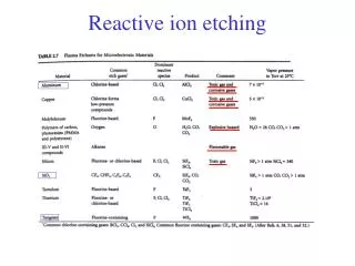
RIE Reactor Materials Since both the electrodes and the walls of the reactor can become sources of sputtered material which may deposit on the wafer being etched, the choice of the wall/electrode materials is of critical importance.The electrode effects can significantly alter the plasma chemistry.Micromasking and surface roughening can be avoided by using electrode materials which form volatile products with the etching gas.
Reaction Steps Transport of plasma-generated reactive intermediates Formation of a DC bias for ion acceleration Active species generation Adsorption Desorption of volatile reaction product Pumpout of volatile reaction product Reaction
RIE Damage • Surface residues • Impurity penetration (implantation, diffusion) • Lattice damage • Dopant loss or loss of dopant activity • Heavy metal contamination • Surface roughness • Gate oxide breakdown or introduction of traps • Mobile ion contamination • Post-RIE corrosion
Deep RIE process flow Deep RIE process of Pyrex glass using SF6 plasma
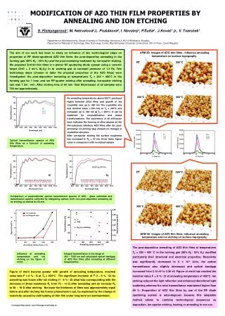
Etching rate vs. Pressure Etch rates as a function of process,self-bias voltage -390 V, etching time 1 h).
Etching rate vs. Pressure SEM images (self-bias voltage -390 V, etching time 1 h).
Etching rate vs. Self-bias Voltage Etch rates as a function of self-bias voltage and the SEM images, pressure 0.2 Pa, etching time 1 h.
Etching rate vs. Self-bias Voltage SEM images: Etch rates as a function of self-bias voltage, pressure 0.2 Pa, etching time 1 h.
Scoop-out Etching The schematic illustration of the scoop-out etching method Honeycomb structure fabricated by the scoop-out etching method: (A) before etching; (B) after etching. The wafer thickness is 200 micrometer and the etching time is 10 h.
Application I-Fabrication of SMA Micropump Micropump structure with SMA actuator: (a) pressurization type and (b) evacuation type.
Process-Fabrication of SMA Micropump After bonding the Pyrex glass cap to the TiNi thin film, the remaining Si layer beneath the TiNi thin film was removed by reactive ion etching (RIE) in SF6 gas. In this etching process, only the remaining Si layer has to be etched, without etching of the TiNi thin film. In order to achieve this, we need to measure the etch rates of Si and TiNi thin film, as well as those of SiO2, Cr and positive photoresist layers as a mask material.
Application II-diamond membranes for MEMS (Up) Schematic diagram of the process flow steps to fabricate CVD diamond membrane. (Right) SEM (a) backside of diamond membrane and (b) typical morphology of the backside of the fabricated diamond membrane using the RIE etching process
Application III-Quartz Crystal Microbalance Schematic illustration of idea of one-chip multichannel QCM sensor Process steps of the multichannel sensor
Modeling • Difficulties • Particle Dynamics • Recent method • Statistical Approach • Neural Network • Advantage for Neural Network Method • Accurate • Robustness • Multi-parameters are included
Modeling Representation of the parameter space in plasma etching. The key internal plasma properties (middle) are the bridge between externally controlled variables (top) and the figures of merit (bottom).
Trend • To enhance plasma generation schemes for high rate low pressure etching; • RIE process-integration (process clustering); • Real-time control of RIE processes; • To improve fundamental understanding and computer models of RIE processes
Summary • RIE is plasma-based dry etching technique; • Etching directionality, selectivity, contaminations and end point etc. are the important issues which must be considered; • The change of pressure, self-bias and stage temperature will result the change of etching rate and etching profile; • RIE is widely used in the Silicon technology in microelectronics field; • The neural network has been developed to simulate the RIE process; • The trend is to improve the understanding and modeling of RIE process in order to achieve the real-time control and enlarge its application.