Download
1 / 11
140 likes | 299 Views
ICL7660 and ICL7660A contain all the necessary circuitry to complete a negative voltage converter, with the exception of 2 external capacitors which may be inexpensive 10μF polarized electrolytic types. Please visit for more information http://www.intersil.com/en/products/power-management/isolated-power/charge-pumps/ICL7660.html

E N D
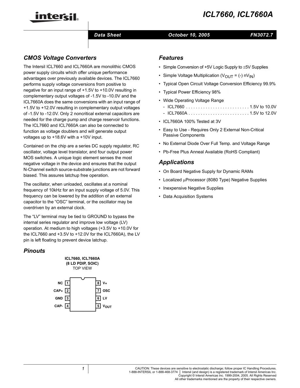
ICL7660, ICL7660A ® Data Sheet October 10, 2005 FN3072.7 CMOS Voltage Converters Features The Intersil ICL7660 and ICL7660A are monolithic CMOS power supply circuits which offer unique performance advantages over previously available devices. The ICL7660 performs supply voltage conversions from positive to negative for an input range of +1.5V to +10.0V resulting in complementary output voltages of -1.5V to -10.0V and the ICL7660A does the same conversions with an input range of +1.5V to +12.0V resulting in complementary output voltages of -1.5V to -12.0V. Only 2 noncritical external capacitors are needed for the charge pump and charge reservoir functions. The ICL7660 and ICL7660A can also be connected to function as voltage doublers and will generate output voltages up to +18.6V with a +10V input. • Simple Conversion of +5V Logic Supply to ±5V Supplies • Simple Voltage Multiplication (VOUT = (-) nVIN) • Typical Open Circuit Voltage Conversion Efficiency 99.9% • Typical Power Efficiency 98% • Wide Operating Voltage Range - ICL7660 . . . . . . . . . . . . . . . . . . . . . . . . . . 1.5V to 10.0V - ICL7660A . . . . . . . . . . . . . . . . . . . . . . . . . 1.5V to 12.0V • ICL7660A 100% Tested at 3V • Easy to Use - Requires Only 2 External Non-Critical Passive Components • No External Diode Over Full Temp. and Voltage Range Contained on the chip are a series DC supply regulator, RC oscillator, voltage level translator, and four output power MOS switches. A unique logic element senses the most negative voltage in the device and ensures that the output N-Channel switch source-substrate junctions are not forward biased. This assures latchup free operation. • Pb-Free Plus Anneal Available (RoHS Compliant) Applications • On Board Negative Supply for Dynamic RAMs • Localized µProcessor (8080 Type) Negative Supplies The oscillator, when unloaded, oscillates at a nominal frequency of 10kHz for an input supply voltage of 5.0V. This frequency can be lowered by the addition of an external capacitor to the “OSC” terminal, or the oscillator may be overdriven by an external clock. • Inexpensive Negative Supplies • Data Acquisition Systems The “LV” terminal may be tied to GROUND to bypass the internal series regulator and improve low voltage (LV) operation. At medium to high voltages (+3.5V to +10.0V for the ICL7660 and +3.5V to +12.0V for the ICL7660A), the LV pin is left floating to prevent device latchup. Pinouts ICL7660, ICL7660A (8 LD PDIP, SOIC) TOP VIEW NC 1 8 V+ 2 7 CAP+ OSC 3 6 GND LV 4 5 CAP- VOUT 1 CAUTION: These devices are sensitive to electrostatic discharge; follow proper IC Handling Procedures. 1-888-INTERSIL or 1-888-468-3774 | Intersil (and design) is a registered trademark of Intersil Americas Inc. Copyright © Intersil Americas Inc. 1999-2004, 2005. All Rights Reserved All other trademarks mentioned are the property of their respective owners.
ICL7660, ICL7660A Ordering Information PART NUMBER TEMP. RANGE (°C) PACKAGE PKG. DWG. # ICL7660CBA* 7660CBA 0 to 70 8 Ld SOIC (N) M8.15 ICL7660CBAZ* (See Note) 7660CBAZ 0 to 70 8 Ld SOIC (N) (Pb-free) M8.15 ICL7660CBAZA* (See Note) 7660CBAZ 0 to 70 8 Ld SOIC (N) (Pb-free) M8.15 ICL7660CPA 7660CPA 0 to 70 8 Ld PDIP E8.3 ICL7660CPAZ ( See Note) 7660CPAZ 0 to 70 8 Ld PDIP** (Pb-free) E8.3 ICL7660ACBA* 7660ACBA 0 to 70 8 Ld SOIC (N) M8.15 ICL7660ACBAZA* (See Note) 7660ACBAZ 0 to 70 8 Ld SOIC (N) (Pb-free) M8.15 ICL7660ACPA 7660ACPA 0 to 70 8 Ld PDIP E8.3 ICL7660ACPAZ (See Note) 7660ACPAZ 0 to 70 8 Ld PDIP** (Pb-free) E8.3 ICL7660AIBA* 7660AIBA -40 to 85 8 Ld SOIC (N) M8.15 ICL7660AIBAZA* (See Note) 7660AIBAZ -40 to 85 8 Ld SOIC (N) (Pb-free) M8.15 *Add “-T” suffix to part number for tape and reel packaging. **Pb-free PDIPs can be used for through hole wave solder processing only. They are not intended for use in Reflow solder processing applications. NOTE: Intersil Pb-free plus anneal products employ special Pb-free material sets; molding compounds/die attach materials and 100% matte tin plate termination finish, which are RoHS compliant and compatible with both SnPb and Pb-free soldering operations. Intersil Pb-free products are MSL classified at Pb-free peak reflow temperatures that meet or exceed the Pb-free requirements of IPC/JEDEC J STD-020. 2 FN3072.7 October 10, 2005
ICL7660, ICL7660A CAbsolute Maximum Ratings Thermal Information θJA (°C/W) 110 160 θJC (°C/W) N/A N/A Supply Voltage ICL7660 . . . . . . . . . . . . . . . . . . . . . . . . . . . . . . . . . . . . . . . +10.5V ICL7660A . . . . . . . . . . . . . . . . . . . . . . . . . . . . . . . . . . . . . . +13.0V LV and OSC Input Voltage. . . . . . -0.3V to (V+ +0.3V) for V+ < 5.5V (Note 2) . . . . . . . . . . . . . . (V+ -5.5V) to (V+ +0.3V) for V+ > 5.5V Current into LV (Note 2). . . . . . . . . . . . . . . . . . . 20µA for V+ > 3.5V Output Short Duration (VSUPPLY≤ 5.5V) . . . . . . . . . . . .Continuous Thermal Resistance (Typical, Note 1) PDIP Package* . . . . . . . . . . . . . . . . . . SOIC Package . . . . . . . . . . . . . . . . . . . Maximum Storage Temperature Range. . . . . . . . . . .-65°C to 150°C Maximum Lead Temperature (Soldering, 10s). . . . . . . . . . . . .300°C (SOIC - Lead Tips Only) *Pb-free PDIPs can be used for through hole wave solder processing only. They are not intended for use in Reflow solder processing applications. Operating Conditions Temperature Range ICL7660C, ICL7660AC. . . . . . . . . . . . . . . . . . . . . . . . 0°C to 70°C ICL7660AI . . . . . . . . . . . . . . . . . . . . . . . . . . . . . . . .-40°C to 85°C CAUTION: Stresses above those listed in “Absolute Maximum Ratings” may cause permanent damage to the device. This is a stress only rating and operation of the device at these or any other conditions above those indicated in the operational sections of this specification is not implied. NOTE: 1. θJA is measured with the component mounted on an evaluation PC board in free air. Electrical Specifications ICL7660 and ICL7660A, V+ = 5V, TA = 25°C, COSC = 0, Test Circuit Figure 11 Unless Otherwise Specified ICL7660 ICL7660A PARAMETER SYMBOL TEST CONDITIONS MIN TYP MAX MIN TYP MAX UNITS RL = ∞ MIN ≤ TA≤ MAX, RL = 10kΩ, LV to GND MIN ≤ TA≤ MAX, RL = 10kΩ, LV to Open µA Supply Current I+ - 170 500 - 80 165 Supply Voltage Range - Lo VL+ 1.5 - 3.5 1.5 - 3.5 V Supply Voltage Range - Hi VH+ 3.0 - 10.0 3 - 12 V Ω Output Source Resistance ROUT IOUT = 20mA, TA = 25°C IOUT = 20mA, 0°C ≤ TA≤ 70°C IOUT = 20mA, -55°C ≤ TA≤ 125°C IOUT = 20mA, -40°C ≤ TA≤ 85°C V+ = 2V, IOUT = 3mA, LV to GND 0°C ≤ TA≤ 70°C - 55 100 - 60 100 Ω - - 120 - - 120 Ω - - 150 - - - Ω - - - - - 120 Ω - - 300 - - 300 Ω V+ = 2V, IOUT = 3mA, LV to GND, -55°C ≤ TA≤ 125°C - - 400 - - - Oscillator Frequency fOSC - 10 - - 10 - kHz RL = 5kΩ RL =∞ Power Efficiency PEF 95 98 - 96 98 - % Voltage Conversion Efficiency VOUT EF 97 99.9 - 99 99.9 - % MΩ Oscillator Impedance ZOSC V+ = 2V - 1.0 - - 1 - kΩ V = 5V - 100 - - - - ICL7660A, V+ = 3V, TA = 25°C, OSC = Free running, Test Circuit Figure 11, Unless Otherwise Specified V+ = 3V, RL = ∞, 25°C µA Supply Current (Note 3) I+ - - - - 26 100 µA 0°C < TA < 70°C - - - - - 125 µA -40°C < TA < 85°C - - - - - 125 Ω Output Source Resistance ROUT V+ = 3V, IOUT = 10mA - - - - 97 150 Ω 0°C < TA < 70°C - - - - - 200 Ω -40°C < TA < 85°C - - - - - 200 Oscillator Frequency (Note 3) fOSC V+ = 3V (same as 5V conditions) - - - 5.0 8 - kHz 0°C < TA < 70°C - - - 3.0 - - kHz -40°C < TA < 85°C - - - 3.0 - - kHz 3 FN3072.7 October 10, 2005
ICL7660, ICL7660A Electrical Specifications ICL7660 and ICL7660A, V+ = 5V, TA = 25°C, COSC = 0, Test Circuit Figure 11 Unless Otherwise Specified (Continued) ICL7660 ICL7660A PARAMETER SYMBOL TEST CONDITIONS MIN TYP MAX MIN TYP MAX UNITS V+ = 3V, RL = ∞ Voltage Conversion Efficiency VOUTEFF - - - 99 - - % TMIN < TA < TMAX V+ = 3V, RL = 5kΩ - - - 99 - - % Power Efficiency PEFF - - - 96 - - % TMIN < TA < TMAX - - - 95 - - % NOTES: 2. Connecting any input terminal to voltages greater than V+ or less than GND may cause destructive latchup. It is recommended that no inputs from sources operating from external supplies be applied prior to “power up” of the ICL7660, ICL7660A. 3. Derate linearly above 50°C by 5.5mW/°C. 4. In the test circuit, there is no external capacitor applied to pin 7. However, when the device is plugged into a test socket, there is usually a very small but finite stray capacitance present, of the order of 5pF. 5. The Intersil ICL7660A can operate without an external diode over the full temperature and voltage range. This device will function in existing designs which incorporate an external diode with no degradation in overall circuit performance. Functional Block Diagram V+ CAP+ VOLTAGE LEVEL TRANSLATOR RC ÷2 OSCILLATOR CAP- VOUT OSC LV VOLTAGE REGULATOR LOGIC NETWORK Typical Performance Curves (Test Circuit of Figure 11) 10 10K TA = 25°C OUTPUT SOURCE RESISTANCE (Ω) 8 SUPPLY VOLTAGE RANGE (NO DIODE REQUIRED) SUPPLY VOLTAGE (V) 1000 6 4 100 2 10 0 0 1 2 3 4 5 6 7 8 -55 -25 0 25 50 100 125 TEMPERATURE (°C) SUPPLY VOLTAGE (V+) FIGURE 1. OPERATING VOLTAGE AS A FUNCTION OF TEMPERATURE FIGURE 2. OUTPUT SOURCE RESISTANCE AS A FUNCTION OF SUPPLY VOLTAGE 4 FN3072.7 October 10, 2005
ICL7660, ICL7660A Typical Performance Curves (Test Circuit of Figure 11) (Continued) 350 100 TA = 25°C POWER CONVERSION EFFICIENCY (%) IOUT = 1mA 98 OUTPUT SOURCE RESISTANCE (Ω) 300 IOUT = 1mA 96 250 94 92 200 IOUT = 15mA 90 V+ = +2V 150 88 86 100 84 50 82 V+ = 5V V+ = +5V 80 0 -55 100 1K 10K -25 0 25 50 75 100 125 OSC. FREQUENCY fOSC (Hz) TEMPERATURE (°C) FIGURE 3. OUTPUT SOURCE RESISTANCE AS A FUNCTION OF TEMPERATURE FIGURE 4. POWER CONVERSION EFFICIENCY AS A FUNCTION OF OSC. FREQUENCY 10K 20 OSCILLATOR FREQUENCY fOSC (kHz) OSCILLATOR FREQUENCY fOSC (Hz) 18 16 1K 14 12 100 10 8 V+ = 5V TA = 25°C V+ = +5V 6 10 -50 -25 0 25 50 75 100 125 1.0 10 100 1000 10K TEMPERATURE (°C) COSC (pF) FIGURE 5. FREQUENCY OF OSCILLATION AS A FUNCTION OF EXTERNAL OSC. CAPACITANCE FIGURE 6. UNLOADED OSCILLATOR FREQUENCY AS A FUNCTION OF TEMPERATURE 5 100 100 TA = 25°C V+ = +5V POWER CONVERSION EFFICIENCY (%) 90 4 90 PEFF I+ 80 80 3 SUPPLY CURRENT I+ (mA) 70 70 2 OUTPUT VOLTAGE 60 60 1 50 50 0 40 40 -1 30 30 -2 20 20 -3 TA = 25°C V+ = +5V 10 10 -4 SLOPE 55Ω 0 0 -5 0 10 20 30 40 50 60 0 10 20 30 40 50 60 70 80 LOAD CURRENT IL (mA) LOAD CURRENT IL (mA) FIGURE 7. OUTPUT VOLTAGE AS A FUNCTION OF OUTPUT CURRENT FIGURE 8. SUPPLY CURRENT AND POWER CONVERSION EFFICIENCY AS A FUNCTION OF LOAD CURRENT 5 FN3072.7 October 10, 2005
ICL7660, ICL7660A Typical Performance Curves (Test Circuit of Figure 11) (Continued) +2 100 20.0 TA = 25°C V+ = 2V POWER CONVERSION EFFICIENCY (%) 90 18.0 SUPPLY CURRENT (mA) (NOTE 6) I+ 80 16.0 +1 PEFF 70 14.0 OUTPUT VOLTAGE 60 12.0 50 10.0 0 40 8.0 30 6.0 -1 20 4.0 TA = 25°C V+ = 2V SLOPE 150Ω 10 2.0 0 0 -2 0 1.5 3.0 4.5 6.0 7.5 9.0 0 1 2 3 4 5 6 7 8 LOAD CURRENT IL (mA) LOAD CURRENT IL (mA) FIGURE 9. OUTPUT VOLTAGE AS A FUNCTION OF OUTPUT CURRENT FIGURE 10. SUPPLY CURRENT AND POWER CONVERSION EFFICIENCY AS A FUNCTION OF LOAD CURRENT NOTE: 6. These curves include in the supply current that current fed directly into the load RL from the V+ (See Figure 11). Thus, approximately half the supply current goes directly to the positive side of the load, and the other half, through the ICL7660/ICL7660A, to the negative side of the load. Ideally, VOUT∼2VIN, IS∼ 2IL, so VIN x IS∼ VOUT x IL. IS V+ (+5V) 1 8 2 7 IL ICL7660 ICL7660A C1 10µF + - 3 6 4 5 RL COSC (NOTE) -VOUT - C2 10µF + NOTE: For large values of COSC (>1000pF) the values of C1 and C2 should be increased to 100µF. FIGURE 11. ICL7660, ICL7660A TEST CIRCUIT Detailed Description The ICL7660 and ICL7660A contain all the necessary circuitry to complete a negative voltage converter, with the exception of 2 external capacitors which may be inexpensive 10µF polarized electrolytic types. The mode of operation of the device may be best understood by considering Figure 12, which shows an idealized negative voltage converter. Capacitor C1 is charged to a voltage, V+, for the half cycle when switches S1 and S3 are closed. (Note: Switches S2 and S4 are open during this half cycle.) During the second half cycle of operation, switches S2 and S4 are closed, with S1 and S3 open, thereby shifting capacitor C1 negatively by V+ volts. Charge is then transferred from C1 to C2 such that the voltage on C2 is exactly V+, assuming ideal switches and no load on C2. The ICL7660 approaches this ideal situation more closely than existing non-mechanical circuits. In the ICL7660 and ICL7660A, the 4 switches of Figure 12 are MOS power switches; S1 is a P-Channel device and S2, S3 and S4 are N-Channel devices. The main difficulty with this approach is that in integrating the switches, the substrates of S3 and S4 must always remain reverse biased with respect to their sources, but not so much as to degrade their “ON” resistances. In addition, at circuit start-up, and under output short circuit conditions (VOUT = V+), the output voltage must be sensed and the substrate bias adjusted accordingly. Failure to accomplish this would result in high power losses and probable device latchup. This problem is eliminated in the ICL7660 and ICL7660A by a logic network which senses the output voltage (VOUT) together with the level translators, and switches the substrates of S3 and S4 to the correct level to maintain necessary reverse bias. 6 FN3072.7 October 10, 2005
ICL7660, ICL7660A The voltage regulator portion of the ICL7660 and ICL7660A is an integral part of the anti-latchup circuitry, however its inherent voltage drop can degrade operation at low voltages. Therefore, to improve low voltage operation the “LV” pin should be connected to GROUND, disabling the regulator. For supply voltages greater than 3.5V the LV terminal must be left open to insure latchup proof operation, and prevent device damage. ENERGY IS LOST ONLY IN THE TRANSFER OF CHARGE BETWEEN CAPACITORS IF A CHANGE IN VOLTAGE OCCURS. The energy lost is defined by: E = 1/2 C1 (V12 - V22) where V1 and V2 are the voltages on C1 during the pump and transfer cycles. If the impedances of C1 and C2 are relatively high at the pump frequency (refer to Figure 12) compared to the value of RL, there will be a substantial difference in the voltages V1 and V2. Therefore it is not only desirable to make C2 as large as possible to eliminate output voltage ripple, but also to employ a correspondingly large value for C1 in order to achieve maximum efficiency of operation. 8 S1 2 S2 VIN C1 3 3 C2 S4 5 S3 Do’s And Don’ts 1. Do not exceed maximum supply voltages. 2. Do not connect LV terminal to GROUND for supply voltages greater than 3.5V. 3. Do not short circuit the output to V+ supply for supply voltages above 5.5V for extended periods, however, transient conditions including start-up are okay. 4. When using polarized capacitors, the + terminal of C1 must be connected to pin 2 of the ICL7660 and ICL7660A and the + terminal of C2 must be connected to GROUND. 5. If the voltage supply driving the ICL7660 and ICL7660A has a large source impedance (25Ω - 30Ω), then a 2.2µF capacitor from pin 8 to ground may be required to limit rate of rise of input voltage to less than 2V/µs. 6. User should insure that the output (pin 5) does not go more positive than GND (pin 3). Device latch up will occur under these conditions. A 1N914 or similar diode placed in parallel with C2 will prevent the device from latching up under these conditions. (Anode pin 5, Cathode pin 3). VOUT = -VIN 7 FIGURE 12. IDEALIZED NEGATIVE VOLTAGE CONVERTER Theoretical Power Efficiency Considerations In theory a voltage converter can approach 100% efficiency if certain conditions are met. 1. The driver circuitry consumes minimal power. 2. The output switches have extremely low ON resistance and virtually no offset. 3. The impedances of the pump and reservoir capacitors are negligible at the pump frequency. The ICL7660 and ICL7660A approach these conditions for negative voltage conversion if large values of C1 and C2 are used. V+ 1 8 RO 2 7 VOUT ICL7660 ICL7660A - + - 10µF 3 6 V+ + 4 5 VOUT = -V+ - 10µF + FIGURE 13A. CONFIGURATION FIGURE 13B. THEVENIN EQUIVALENT FIGURE 13. SIMPLE NEGATIVE CONVERTER 7 FN3072.7 October 10, 2005
ICL7660, ICL7660A t1 t2 B 0 V A -(V+) FIGURE 14. OUTPUT RIPPLE V+ 1 8 2 7 ICL7660 ICL7660A “1” 1 8 3 6 C1 RL 2 7 ICL7660 ICL7660A “n” 4 5 3 6 C1 4 5 - C2 + FIGURE 15. PARALLELING DEVICES V+ 1 8 ICL7660 ICL7660A “1” 2 7 1 8 + - 10µF 3 6 2 7 ICL7660 ICL7660A “n” + - 4 5 10µF 3 6 VOUT = -nV+ 4 5 10µF - - + 10µF + FIGURE 16. CASCADING DEVICES FOR INCREASED OUTPUT VOLTAGE Typical Applications RO≅ 2(RSW1 + RSW3 + ESRC1) + 1 Simple Negative Voltage Converter The majority of applications will undoubtedly utilize the ICL7660 and ICL7660A for generation of negative supply voltages. Figure 13 shows typical connections to provide a negative supply negative (GND) for supply voltages below 3.5V. + ESRC2 (fPUMP) (C1) fOSC 2 (fPUMP = , RSWX = MOSFET switch resistance) Combining the four RSWX terms as RSW, we see that: 1 RO≅ + 4 (ESRC1) + ESRC2 2 (RSW) + (fPUMP) (C1) The output characteristics of the circuit in Figure 13A can be approximated by an ideal voltage source in series with a resistance as shown in Figure 13B. The voltage source has a value of -V+. The output impedance (RO) is a function of the ON resistance of the internal MOS switches (shown in Figure 12), the switching frequency, the value of C1 and C2, and the ESR (equivalent series resistance) of C1 and C2. A good first order approximation for RO is: RSW, the total switch resistance, is a function of supply voltage and temperature (See the Output Source Resistance graphs), typically 23Ω at 25°C and 5V. Careful selection of C1 and C2 will reduce the remaining terms, minimizing the output impedance. High value capacitors will reduce the 1/(fPUMP• C1) component, and low ESR capacitors will lower the ESR term. Increasing the oscillator frequency will reduce the 1/(fPUMP• C1) term, but may have the side effect of a net increase in output impedance when C1 > 10µF and there is no longer enough time to fully charge the capacitors RO≅ 2(RSW1 + RSW3 + ESRC1) + 2(RSW2 + RSW4 + ESRC1) + 8 FN3072.7 October 10, 2005
ICL7660, ICL7660A Cascading Devices The ICL7660 and ICL7660A may be cascaded as shown to produced larger negative multiplication of the initial supply voltage. However, due to the finite efficiency of each device, the practical limit is 10 devices for light loads. The output voltage is defined by: every cycle. In a typical application where fOSC = 10kHz and C = C1 = C2 = 10µF: 1 RO≅ 2 (23) + + 4 (ESRC1) + ESRC2 (5 • 103) (10-5) RO≅ 46 + 20 + 5 (ESRC) VOUT = -n (VIN), Since the ESRs of the capacitors are reflected in the output impedance multiplied by a factor of 5, a high value could potentially swamp out a low 1/(fPUMP• C1) term, rendering an increase in switching frequency or filter capacitance ineffective. Typical electrolytic capacitors may have ESRs as high as 10Ω. where n is an integer representing the number of devices cascaded. The resulting output resistance would be approximately the weighted sum of the individual ICL7660 and ICL7660A ROUT values. 1 Changing the ICL7660/ICL7660A Oscillator Frequency It may be desirable in some applications, due to noise or other considerations, to increase the oscillator frequency. This is achieved by overdriving the oscillator from an external clock, as shown in Figure 17. In order to prevent possible device latchup, a 1kΩ resistor must be used in series with the clock output. In a situation where the designer has generated the external clock frequency using TTL logic, the addition of a 10kΩ pullup resistor to V+ supply is required. Note that the pump frequency with external clocking, as with internal clocking, will be 1/2 of the clock frequency. Output transitions occur on the positive-going edge of the clock. RO≅ 2 (23) + + 4 (ESRC1) + ESRC2 (5 • 103) (10-5) RO/≅ 46 + 20 + 5 (ESRC) Since the ESRs of the capacitors are reflected in the output impedance multiplied by a factor of 5, a high value could potentially swamp out a low 1/(fPUMP• C1) term, rendering an increase in switching frequency or filter capacitance ineffective. Typical electrolytic capacitors may have ESRs as high as 10Ω. Output Ripple ESR also affects the ripple voltage seen at the output. The total ripple is determined by 2 voltages, A and B, as shown in Figure 14. Segment A is the voltage drop across the ESR of C2 at the instant it goes from being charged by C1 (current flow into C2) to being discharged through the load (current flowing out of C2). The magnitude of this current change is 2• IOUT, hence the total drop is 2• IOUT• eSRC2V. Segment B is the voltage change across C2 during time t2, the half of the cycle when C2 supplies current to the load. The drop at B is lOUT • t2/C2V. The peak-to-peak ripple voltage is the sum of these voltage drops: ≅ [ V+ V+ 1 8 1kΩ CMOS GATE 2 7 ICL7660 ICL7660A + - 10µF 3 6 4 5 VOUT - 10µF + + 2 (ESRC2)]IOUT 1 VRIPPLE 2 (fPUMP) (C2) FIGURE 17. EXTERNAL CLOCKING Again, a low ESR capacitor will reset in a higher performance output. It is also possible to increase the conversion efficiency of the ICL7660 and ICL7660A at low load levels by lowering the oscillator frequency. This reduces the switching losses, and is shown in Figure 18. However, lowering the oscillator frequency will cause an undesirable increase in the impedance of the pump (C1) and reservoir (C2) capacitors; this is overcome by increasing the values of C1 and C2 by the same factor that the frequency has been reduced. For example, the addition of a 100pF capacitor between pin 7 (OSC) and V+ will lower the oscillator frequency to 1kHz from its nominal frequency of 10kHz (a multiple of 10), and thereby necessitate a corresponding increase in the value of C1 and C2 (from 10µF to 100µF). Paralleling Devices Any number of ICL7660 and ICL7660A voltage converters may be paralleled to reduce output resistance. The reservoir capacitor, C2, serves all devices while each device requires its own pump capacitor, C1. The resultant output resistance would be approximately: ROUT (of ICL7660/ICL7660A) n (number of devices) ROUT = 9 FN3072.7 October 10, 2005
ICL7660, ICL7660A V+ V+ VOUT = - (nVIN - VFDX) 1 8 1 8 COSC - 2 7 2 7 ICL7660 ICL7660A ICL7660 ICL7660A C3 D1 + - + + - C1 3 6 3 6 C1 4 5 VOUT - 4 5 VOUT = (2V+) - (VFD1) - (VFD2) C2 + D2 - + +- C4 C2 FIGURE 18. LOWERING OSCILLATOR FREQUENCY Positive Voltage Doubling The ICL7660 and ICL7660A may be employed to achieve positive voltage doubling using the circuit shown in Figure 19. In this application, the pump inverter switches of the ICL7660 and ICL7660A are used to charge C1 to a voltage level of V+ -VF (where V+ is the supply voltage and VF is the forward voltage drop of diode D1). On the transfer cycle, the voltage on C1 plus the supply voltage (V+) is applied through diode D2 to capacitor C2. The voltage thus created on C2 becomes (2V+) - (2VF) or twice the supply voltage minus the combined forward voltage drops of diodes D1 and D2. FIGURE 20. COMBINED NEGATIVE VOLTAGE CONVERTER AND POSITIVE DOUBLER Voltage Splitting The bidirectional characteristics can also be used to split a higher supply in half, as shown in Figure 21. The combined load will be evenly shared between the two sides. Because the switches share the load in parallel, the output impedance is much lower than in the standard circuits, and higher currents can be drawn from the device. By using this circuit, and then the circuit of Figure 16, +15V can be converted (via +7.5, and -7.5) to a nominal -15V, although with rather high series output resistance (~250Ω). The source impedance of the output (VOUT) will depend on the output current, but for V+ = 5V and an output current of 10mA it will be approximately 60Ω. V+ + - V+ 50µF RL1 1 8 1 8 D1 2 7 ICL7660 ICL7660A VOUT =V+ - V- 2 7 ICL7660 ICL7660A VOUT = (2V+) - (2VF) 2 3 6 + - D2 50µF 3 6 RL2 4 5 4 5 + - + - + - C1 C2 50µF V- FIGURE 19. POSITIVE VOLT DOUBLER FIGURE 21. SPLITTING A SUPPLY IN HALF Combined Negative Voltage Conversion and Positive Supply Doubling Figure 20 combines the functions shown in Figures 13 and Figure 19 to provide negative voltage conversion and positive voltage doubling simultaneously. This approach would be, for example, suitable for generating +9V and -5V from an existing +5V supply. In this instance capacitors C1 and C3 perform the pump and reservoir functions respectively for the generation of the negative voltage, while capacitors C2 and C4 are pump and reservoir respectively for the doubled positive voltage. There is a penalty in this configuration which combines both functions, however, in that the source impedances of the generated supplies will be somewhat higher due to the finite impedance of the common charge pump driver at pin 2 of the device. Regulated Negative Voltage Supply In some cases, the output impedance of the ICL7660 and ICL7660A can be a problem, particularly if the load current varies substantially. The circuit of Figure 22 can be used to overcome this by controlling the input voltage, via an ICL7611 low-power CMOS op amp, in such a way as to maintain a nearly constant output voltage. Direct feedback is inadvisable, since the ICL7660s and ICL7660As output does not respond instantaneously to change in input, but only after the switching delay. The circuit shown supplies enough delay to accommodate the ICL7660 and ICL7660A, while maintaining adequate feedback. An increase in pump and storage capacitors is desirable, and the values shown provides an output impedance of less than 5Ω to a load of 10mA. 10 FN3072.7 October 10, 2005
ICL7660, ICL7660A Other Applications Further information on the operation and use of the ICL7660 and ICL7660A may be found in AN051 “Principals and Applications of the ICL7660 and ICL7660A CMOS Voltage Converter”. 50K +8V 56K +8V -10µF 100Ω 50K + - ICL7611 + 100K 1 8 2 7 ICL7660 ICL7660A + - ICL8069 100µF 3 6 4 5 VOUT - 800K 250K VOLTAGE ADJUST 100µF + FIGURE 22. REGULATING THE OUTPUT VOLTAGE +5V LOGIC SUPPLY 12 11 TTL DATA INPUT 16 1 4 3 RS232 DATA OUTPUT +5V -5V 15 1 8 IH5142 2 7 ICL7660 ICL7660A + - 13 14 3 6 10µF 4 5 - 10µF + FIGURE 23. RS232 LEVELS FROM A SINGLE 5V SUPPLY All Intersil U.S. products are manufactured, assembled and tested utilizing ISO9000 quality systems. Intersil Corporation’s quality certifications can be viewed at www.intersil.com/design/quality Intersil products are sold by description only. Intersil Corporation reserves the right to make changes in circuit design, software and/or specifications at any time without notice. Accordingly, the reader is cautioned to verify that data sheets are current before placing orders. Information furnished by Intersil is believed to be accurate and reliable. However, no responsibility is assumed by Intersil or its subsidiaries for its use; nor for any infringements of patents or other rights of third parties which may result from its use. No license is granted by implication or otherwise under any patent or patent rights of Intersil or its subsidiaries. For information regarding Intersil Corporation and its products, see www.intersil.com 11 FN3072.7 October 10, 2005