Slide Note
0 likes | 10 Views
The Boltzmann relation, quasi-Fermi levels, and current-voltage characteristics of semiconductor junctions are explored in this detailed discourse. The analysis delves into the electron and hole current densities, depletion region properties, and the Shockley equation governing diode behavior. Additionally, the history and functioning of light-emitting diodes (LEDs) are discussed, highlighting their ability to emit light under forward-biased conditions in various regions of the spectrum.

E N D
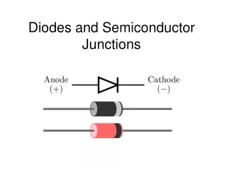
CURRENT CURRENT- -VOLTAGE CHARACTERISTICS VOLTAGE CHARACTERISTICS • We first consider the Boltzmann relation. At thermal equilibrium this relation is given by • At thermal equilibrium, the pn product from the above equations is equal to ni2. • When voltage is applied, the minority-carrier densities on both sides of the junction are changed, and the pn product is no longer equal to ni2.
• We shall now define the quasi-Fermi levels as follows: • where EFnand EFpare the quasi-Fermi levels for electrons and holes, respectively.
• For a forward bias, (EFn- EFp) > 0 and pn > ni2; on the other hand, for a reversed bias, (EFn- EFp) < 0 and pn < ni2. • From the continuity equation we introduced last time (Without generation and recombination), we now have:
• Thus, the electron and hole current densities are proportional to the gradients of the electron and hole quasi-Fermi levels, respectively. • If EFn= EFp= constant (at thermal equilibrium), then Jn= Jp= 0.
• Inside the depletion region, EFnand EFpremain relatively constant. • This comes about because the carrier concentrations are relatively much higher inside the depletion region, but since the currents remain fairly constant, the gradients of the quasi-Fermi levels have to be small. • In addition, the depletion width is typically much shorter than the diffusion length, so the total drop of quasi-Fermi levels inside the depletion width is not significant. • With these arguments, it follows that within the depletion region,
• Equations 49 and 52 can be combined to give the electron density at the boundary of the depletion-layer region on the p-side (x = - WDp): • where pp≈ pp0for low-level injection, and np0is the equilibrium electron density on the p-side. • In the p region, the equilibrium density of minority carriers, electrons, is the pre-factor that determines the electron density.
• Similarly, • From the continuity equations we obtain for the steady-state condition in the n-side of the junction:
• In these equations, U is the net recombination rate. • Note that due to charge neutrality, majority carriers need to adjust their concentrations such that (nn– nn0) = (pn– pn0). • It also follows that dnn/dx = dpn/dx. • Multiplying Eq. 54a by μppn, and Eq. 54b by μnnn, and combining with the Einstein relation D = (kT/q) μ, we obtain
• Where • Is the ambipolar diffusion coefficient. • And life time of holes: • From the low-injection assumption [e.g., pn<< (nn≈ nn0) in the n-type semiconductor], Eq. 55 reduces to
• In neutral region, no electric field is there: • The solution is
• At x = WDn, the hole diffusion current is • Similarly, we can obtain the electron diffusion current in the p type region:
• The minority-carrier densities and the current densities for the forward-bias and reverse-bias conditions are shown in Fig. 9. • It is interesting to note that the hole current is due to injection of holes from the p-side to the n-side, but the magnitude is determined by the properties in the n-side only • The analogy holds for the electron current. • The total current: • Equation 63 is Shockley equation! Ideal diode law.
• In the forward direction (positive bias on the p-side) for V > 3kT/q, the rate of current rise is constant (Fig. lob); • at 300 K for every decade change of current, the voltage changes by 59.5 mV (= 2.3kTlq). • In the reverse direction, the current density saturates at – J0.
• The Shockley equation adequately predicts the current-voltage characteristics of germanium p-n junctions at low current densities. • For Si and GaAs p-n junctions, however, the ideal equation can only give qualitative agreement. • The departures from the ideal are mainly due to: • (1) the generation and recombination of carriers in the depletion layer, • (2) the high-injection condition that may occur even at relatively small forward bias, • (3) the parasitic IR drop due to series resistance, • (4) the tunneling of carriers between states in the bandgap, • and (5) the surface effects. • In addition, under sufficiently larger field in the reverse direction, the junction will breakdown as a result, for example, of avalanche multiplication.
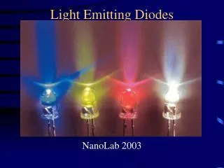
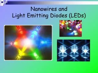
Light emitting diodes • The light-emitting diode, commonly known as LED, is a semiconductor p-n junction that under proper forward-biased conditions can emit external spontaneous radiation in the ultraviolet, visible, and infrared regions of the spectrum. • Electro-luminescence was first discovered by Round as early as 1907 in a contact to a SiC substrate, but was reported only in a short note. • More-detailed experiments were presented by Lossev, whose work spanned from the 1920s to the 1930s.
• After the development of the p-n junction in 1949, LED structures changed from point contacts to p-n junctions. • Other semiconductor materials besides SiC were subsequently studied, such as Ge and Si. • Since these semiconductors have indirect energy gap, their efficiencies were very limited. • Much-higher quantum efficiencies were reported from direct- bandgap GaAs in 1962.
• These studies quickly led to the realization of the semiconductor laser later the same year. • Up to that point, it was considered imperative to use directbandgap material for efficient electroluminescence. • Significant advancement was made on indirect-bandgap materials during 1964- 1965 by introducing isoelectronic impurities. • These studies had a profound impact on commercial LEDs made from indirect- bandgap GaAsP and GaP. • Most recently, a major advancement was made when InGaN was used to produce blue and UV portion of the spectrum which had not been possible before. • This technological advancement not only improves greatly on the realization and performance of white-light LEDs, it also helps to lift the popularity of LEDs as a whole.
• The applications of LEDs are very wide and can be categorized into three kinds. • The first is for display. Typical day-to-day examples are panel displays in different electronic equipments for audio and video home entertainment, panel displays in automobiles, computer screens, calculators, clocks, watches, outdoor signs, traffic lights. • Chances are everybody looks at some LED display everyday.
• The second category is for illumination, replacing the traditional incandescent light bulbs. • Examples in this category are household lamps, flashlight, book light, automobile headlights, etc. • The big advantage here is their high efficiencies, extending the battery life many times in portable usage. • In addition, LEDs are more reliable and have longer lifetime. • This feature greatly reduces the cost of having to replace traditional light bulbs, especially important in outdoor applications such as traffic lights.
• The third application is as light source for optical-fiber communication systems, for low and medium data rates (< 1 Gb/s), over short and medium distances (< 10 km). • Infrared LEDs are more suitable for this application since the wavelength ensures minimum loss in typical optical fibers. • There are advantages and disadvantages to using LEDs as an optical source compared to semiconductor lasers. • The advantages of LEDs include higher-temperature operation, smaller temperature dependence of emitted power, simpler device construction, and simpler drive circuit. • The disadvantages are lower brightness and lower modulation frequency, and wide spectral line width, typically 5 to 20 nm as compared to the narrow line width, 0.1 to 1 angstrom, of a laser.
Device Structures Device Structures • The basic structure of an LED is a p-n junction. • Under forward bias, minority carriers are injected from both sides of the junction. • At the vicinity of the junction, there is an excess of carriers over their equilibrium values (pn > ni2), and recombination will take place. • However, if a heterojunction is utilized in the design, the efficiency can be much improved.
Materials of Choice Materials of Choice • The spectrum covers most of the visible and extends into the infrared region. • For display applications, since the human eye is only sensitive to light of energy greater than 1.8 eV, semiconductors of interest must have energy bandgaps larger than this value. • In general, all of these semiconductors are direct-bandgap materials except for some of the alloy composition in the GaAsP system. • Direct-bandgap semiconductors are particularly important for electroluminescent devices, because the radiative recombination is a first- order transition process (no phonon involved) and the quantum efficiency is expected to be much higher than that for an indirect-bandgap semiconductor, where a phonon is involved.
Definitions of Efficiencies Definitions of Efficiencies • The main function of an LED is to convert electrical energy into light in the visible part of the spectrum for display and illumination purposes. • Knowing the origins of these efficiencies, optimization can be made accordingly.
Internal Quantum Efficiency. Internal Quantum Efficiency. • For a given input power, the radiative recombination processes are in direct competition with the nonradiative ones. • Each of the band-to band transitions and transitions via traps can be either radiative or nonradiative. • Examples of nonradiative band-to-band recombination are those in indirect-bandgap semiconductors. • Conversely, examples of radiative recombination via traps are those via isoelectronic levels.
• The internal quantum efficiency ηin, is the efficiency of converting carrier current to photons, defined as • It can be related to the fraction of the injected carriers that combine radiatively to the total recombination rate, and may also be written in terms of their lifetimes as
• For low-level injection, the radiative recombination rate in the p-side of the junction is given by • Recis the recombination coefficient and Δn is the excess carrier which is much larger than the minority carrier density in equilibrium.
• For low-level injection (Δn <pp0), the radiative lifetime is related to the recombination coefficient by • The nonradiative lifetime is usually attributed to traps (of density Nt) or recombination centers, • where σ is the capture cross section. • It is evident that the radiative lifetime needs to be small to yield high internal quantum efficiency.
External Quantum Efficiency. External Quantum Efficiency. • Obviously for LED applications, what matters is the light emitted external to the device. • For this, the optics inside and outside the device has to be considered. • The parameter to measure the efficiency of getting the light out externally is the optical efficiency , sometimes called the extraction efficiency. • With this factored in, the net external quantum efficiency is defined as
• The optical efficiency is a subject of optics inside and around the devices, totally independent of electrical phenomena. For more details, please read the reference book on page 615.